NPN − MPS8099; PNP − MPS8599
Preferred Device
Amplifier Transistors
Voltage and Current are Negative for PNP Transistors...
NPN − MPS8099; PNP − MPS8599
Preferred Device
Amplifier Transistors
Voltage and Current are Negative for PNP Transistors
Features
Pb−Free Packages are Available*
MAXIMUM RATINGS
Rating Collector −Emitter
Voltage Collector −Base
Voltage Emitter −Base
Voltage Collector Current − Continuous Total Device Dissipation @ TA = 25°C Derate above 25°C
Symbol VCEO VCBO VEBO
IC PD
Value 80 80 4.0 500 625 5.0
Unit Vdc
Vdc
Vdc
mAdc mW mW/°C
Total Device Dissipation @ TC = 25°C PD 1.5 W
Derate above 25°C
12 mW/°C
Operating and Storage Junction Temperature Range
TJ, Tstg −55 to +150 °C
THERMAL CHARACTERISTICS
Characteristic
Symbol
Max
Unit
Thermal Resistance, Junction−to−Ambient (Note 1)
RqJA
200 °C/W
Thermal Resistance, Junction−to−Case
RqJC
83.3 °C/W
Stresses exceeding Maximum Ratings may damage the device. Maximum Ratings are stress ratings only. Functional operation above the Recommended Operating Conditions is not implied. Extended exposure to stresses above the Recommended Operating Conditions may affect device reliability. 1. RqJA is measured with the device soldered into a typical printed circuit board.
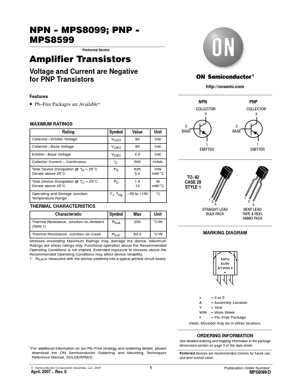
http://onsemi.com
NPN COLLECTOR
3
2 BASE
1 EMITTER
PNP COLLECTOR
3
2 BASE
1 EMITTER
TO−92 CASE 29 STYLE 1
123 STRAIGHT LEAD
BULK PACK
1 2 3
BENT LEAD TAPE & REEL AMMO PACK
MARKING DIAGRAM
MPS 8x99 AYWW G
G
*For additional information on our Pb−Free strategy and soldering details, please download the ON Semiconductor Soldering and Mounting Techniques Ref...