Freescale Semiconductor Technical Data
RF Power Field Effect Transistors
N--Channel Enhancement--Mode Lateral MOSFETs
De...
Freescale Semiconductor Technical Data
RF Power Field Effect Transistors
N--Channel Enhancement--Mode Lateral
MOSFETs
Designed for W--CDMA base station applications with frequencies from 2110 to 2170 MHz. Suitable for TDMA, CDMA and multicarrier amplifier applications. To be used in Class AB for PCN--PCS/cellular radio and WLL applications.
Typical 2--carrier W--CDMA Performance: VDD = 28 Volts, IDQ = 1200 mA, Pout = 30 Watts Avg., f = 2112.5 MHz, Channel Bandwidth = 3.84 MHz, PAR = 8.5 dB @ 0.01% Probability on CCDF. Power Gain — 15.5 dB Drain Efficiency — 27.5% IM3 @ 10 MHz Offset — --37 dBc in 3.84 MHz Channel Bandwidth ACPR @ 5 MHz Offset — --41 dBc in 3.84 MHz Channel Bandwidth
Capable of Handling 10:1 VSWR, @ 28 Vdc, 2140 MHz, 140 Watts CW Output Power
Features
Characterized with Series Equivalent Large--Signal Impedance Parameters Internally Matched for Ease of Use Qualified Up to a Maximum of 32 VDD Operation Integrated ESD Protection Optimized for Doherty Applications RoHS Compliant In Tape and Reel. R3 Suffix = 250 Units per 56 mm, 13 inch Reel.
Document Number: MRF6S21140H Rev. 5, 2/2010
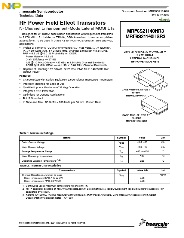
MRF6S21140HR3 MRF6S21140HSR3
2110--2170 MHz, 30 W AVG., 28 V 2 x W--CDMA
LATERAL N--CHANNEL RF POWER
MOSFETs
CASE 465B--03, STYLE 1 NI--880
MRF6S21140HR3
CASE 465C--02, STYLE 1 NI--880S
MRF6S21140HSR3
Table 1. Maximum Ratings
Rating
Symbol
Value
Unit
Drain--Source
Voltage Gate--Source
Voltage Storage Temperature Range Case Operating Temperature Operating J...