Freescale Semiconductor Technical Data
Document Number: MRF6S27050H Rev. 1, 12/2008
www.DataSheet4U.com
RF Power Field...
Freescale Semiconductor Technical Data
Document Number: MRF6S27050H Rev. 1, 12/2008
www.DataSheet4U.com
RF Power Field Effect Transistors
N - Channel Enhancement - Mode Lateral
MOSFETs
Designed for CDMA base station applications with frequencies from 2500 to 2700 MHz. Suitable for WiMAX, WiBro, BWA, and OFDM multicarrier Class AB and Class C amplifier applications. Typical Single - Carrier W - CDMA Performance: VDD = 28 Volts, IDQ = 500 mA, Pout = 7 Watts Avg., f = 2615 MHz, Channel Bandwidth = 3.84 MHz. PAR = 8.5 dB @ 0.01% Probability on CCDF. Power Gain — 16 dB Drain Efficiency — 22.5% ACPR @ 5 MHz Offset — - 42.5 dBc @ 3.84 MHz Channel Bandwidth Capable of Handling 10:1 VSWR, @ 28 Vdc, 2600 MHz, 50 Watts CW Output Power Features Characterized with Series Equivalent Large - Signal Impedance Parameters Internally Matched for Ease of Use Qualified Up to a Maximum of 32 VDD Operation Integrated ESD Protection Designed for Lower Memory Effects and Wide Instantaneous Bandwidth Applications RoHS Compliant In Tape and Reel. R3 Suffix = 250 Units per 56 mm, 13 inch Reel.
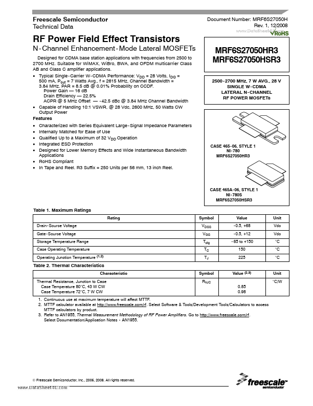
MRF6S27050HR3 MRF6S27050HSR3
2500 - 2700 MHz, 7 W AVG., 28 V SINGLE W - CDMA LATERAL N - CHANNEL RF POWER
MOSFETs
CASE 465 - 06, STYLE 1 NI - 780 MRF6S27050HR3
CASE 465A - 06, STYLE 1 NI - 780S MRF6S27050HSR3
Table 1. Maximum Ratings
Rating Drain - Source
Voltage Gate - Source
Voltage Storage Temperature Range Case Operating Temperature Operating Junction Temperature
(1,2)
Symbol VDSS VGS...