NXP Semiconductors Technical Data
RF Power Field Effect Transistors
N--Channel Enhancement--Mode Lateral MOSFETs
Designe...
NXP Semiconductors Technical Data
RF Power Field Effect Transistors
N--Channel Enhancement--Mode Lateral
MOSFETs
Designed primarily for CW large--signal output and driver applications with frequencies up to 450 MHz. Devices are unmatched and are suitable for use in industrial, medical and scientific applications. Typical CW performance at 220 MHz: VDD = 50 Vdc, IDQ = 30 mA,
Pout = 10 W Power gain — 23.9 dB Drain efficiency — 62%
Capable of handling 10:1 VSWR @ 50 Vdc, 220 MHz, 10 W CW output power
Features Characterized with series equivalent large--signal impedance parameters Qualified up to a maximum of 50 VDD operation Integrated ESD protection 225C capable plastic package
Document Number: MRF6V2010N Rev. 6, 9/2016
MRF6V2010N MRF6V2010NB MRF6V2010GN
10--450 MHz, 10 W, 50 V LATERAL N--CHANNEL
BROADBAND RF POWER
MOSFETs
TO--270--2 PLASTIC MRF6V2010N
TO--272--2 PLASTIC MRF6V2010NB
TO--270G--2 PLASTIC
MRF6V2010GN
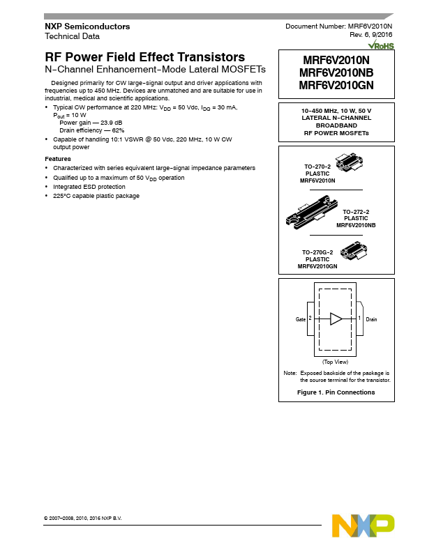
Gate 2
1 Drain
(Top View) Note: Exposed backside of the package is
the source terminal for the transistor.
Figure 1. Pin Connections
2007–2008, 2010, 2016 NXP B.V.
RF Device Data NXP Semiconductors
MRF6V2010N MRF6V2010NB MRF6V2010GN 1
Table 1. Maximum Ratings
Rating
Symbol
Value
Unit
Drain--Source
Voltage Gate--Source
Voltage Storage Temperature Range Case Operating Temperature Operating Junction Temperature (1,2)
Table 2. Thermal Characteristics
Characteristic
VDSS VGS Tstg TC TJ
Symbol
--0.5, +110 --0.5, +10 -- 65 to +150
150 225
Value ...