Freescale Semiconductor Technical Data
RF Power Field--Effect Transistors
N--Channel Enhancement--Mode Lateral MOSFETs
D...
Freescale Semiconductor Technical Data
RF Power Field--Effect Transistors
N--Channel Enhancement--Mode Lateral
MOSFETs
Designed primarily for CW large--signal output and driver applications with frequencies up to 450 MHz. Devices are unmatched and are suitable for use in industrial, medical and scientific applications. Typical CW Performance at 220 MHz: VDD = 50 Volts, IDQ = 450 mA,
Pout = 150 Watts Power Gain — 25 dB Drain Efficiency — 68.3%
Capable of Handling 10:1 VSWR, @ 50 Vdc, 220 MHz, 150 Watts CW Output Power
Features Characterized with Series Equivalent Large--Signal Impedance Parameters Qualified Up to a Maximum of 50 VDD Operation Integrated ESD Protection 225°C Capable Plastic Package RoHS Compliant In Tape and Reel. R1 Suffix = 500 Units per 44 mm, 13 inch Reel.
Document Number: MRF6V2150N Rev. 4, 4/2010
MRF6V2150NR1 MRF6V2150NBR1
10--450 MHz, 150 W, 50 V LATERAL N--CHANNEL
SINGLE--ENDED BROADBAND
RF POWER
MOSFETs
CASE 1486--03, STYLE 1 TO--270 WB--4 PLASTIC MRF6V2150NR1
CASE 1484--04, STYLE 1 TO--272 WB--4 PLASTIC
MRF6V2150NBR1
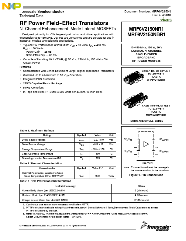
PARTS ARE SINGLE--ENDED
Table 1. Maximum Ratings
Rating Drain--Source
Voltage Gate--Source
Voltage Storage Temperature Range Case Operating Temperature Operating Junction Temperature (1,2)
Table 2. Thermal Characteristics
Characteristic Thermal Resistance, Junction to Case
Case Temperature 80°C, 150 W CW
Symbol VDSS VGS Tstg TC TJ
Value
Unit
-- 0.5, +110 Vdc
-- 0.5, + 12 Vdc
-- 65 to +150 °C
150
°C
225
°C
Sy...