www.DataSheet4U.com
Freescale Semiconductor Technical Data
Document Number: Order from RF Marketing Rev. 4, 10/2006
R...
www.DataSheet4U.com
Freescale Semiconductor Technical Data
Document Number: Order from RF Marketing Rev. 4, 10/2006
RF Power Field Effect Transistor
N - Channel Enhancement - Mode Lateral
MOSFETs
Designed primarily for pulsed wideband large - signal output and driver applications with frequencies up to 450 MHz. Devices are unmatched and are suitable for use in industrial, medical and scientific applications. Typical CW Performance at 220 MHz: VDD = 50 Volts, IDQ = 900 mA, Pout = 300 Watts Power Gain — 27 dB Drain Efficiency — 68% Capable of Handling 10:1 VSWR, @ 50 Vdc, 210 MHz, 300 Watts CW Output Power Features Integrated ESD Protection Greater Negative Gate - Source
Voltage Range for Improved Class C Operation Excellent Thermal Stability Facilitates Manual Gain Control, ALC and Modulation Techniques 225°C Capable Plastic Package RoHS Compliant
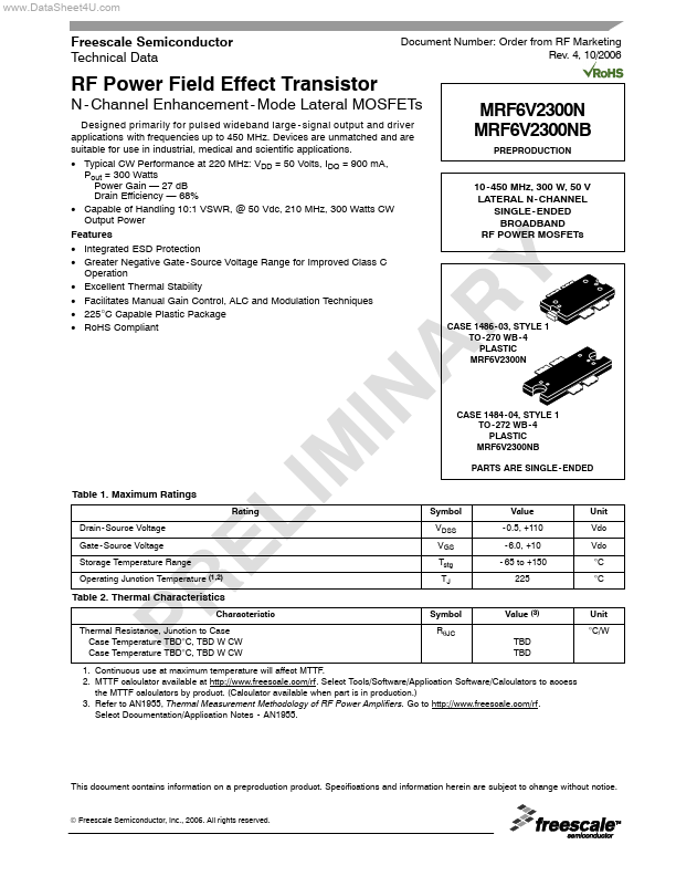
MRF6V2300N MRF6V2300NB
PREPRODUCTION
10 - 450 MHz, 300 W, 50 V LATERAL N - CHANNEL SINGLE - ENDED BROADBAND RF POWER
MOSFETs
CASE 1486 - 03, STYLE 1 TO - 270 WB - 4 PLASTIC MRF6V2300N
CASE 1484 - 04, STYLE 1 TO - 272 WB - 4 PLASTIC MRF6V2300NB PARTS ARE SINGLE - ENDED
Table 1. Maximum Ratings
Rating Drain - Source
Voltage Gate - Source
Voltage Storage Temperature Range Operating Junction Temperature (1,2) Symbol VDSS VGS Tstg TJ Value - 0.5, +110 - 6.0, +10 - 65 to +150 225 Unit Vdc Vdc °C °C
Table 2. Thermal Characteristics
Characteristic Thermal Resistance, Junction to Case Case Temperature TBD°C, TBD W CW...