Freescale Semiconductor Technical Data
RF Power Field Effect Transistors
N--Channel Enhancement--Mode Lateral MOSFETs
De...
Freescale Semiconductor Technical Data
RF Power Field Effect Transistors
N--Channel Enhancement--Mode Lateral
MOSFETs
Designed primarily for CW large--signal output and driver applications with frequencies up to 600 MHz. Devices are unmatched and are suitable for use in industrial, medical and scientific applications.
Typical CW Performance: VDD = 50 Volts, IDQ = 900 mA, Pout = 300 Watts, f = 450 MHz Power Gain — 22 dB Drain Efficiency — 60%
Capable of Handling 10:1 VSWR, @ 50 Vdc, 450 MHz, 300 Watts CW Output Power
Features
Characterized with Series Equivalent Large--Signal Impedance Parameters Qualified Up to a Maximum of 50 VDD Operation Integrated ESD Protection Greater Negative Gate--Source
Voltage Range for Improved Class C
Operation 225°C Capable Plastic Package RoHS Compliant In Tape and Reel. R1 Suffix = 500 Units per 44 mm, 13 inch Reel.
Document Number: MRF6V4300N Rev. 3, 4/2010
MRF6V4300NR1 MRF6V4300NBR1
10--600 MHz, 300 W, 50 V LATERAL N--CHANNEL
SINGLE--ENDED BROADBAND
RF POWER
MOSFETs
CASE 1486--03, STYLE 1 TO--270 WB--4 PLASTIC MRF6V4300NR1
CASE 1484--04, STYLE 1 TO--272 WB--4 PLASTIC
MRF6V4300NBR1 PARTS ARE SINGLE--ENDED
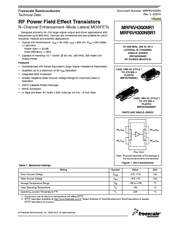
RFin/VGS RFin/VGS
RFout/VDS RFout/VDS
Table 1. Maximum Ratings
(Top View) Note: Exposed backside of the package is
the source terminal for the transistor.
Figure 1. Pin Connections
Rating
Symbol
Value
Unit
Drain--Source
Voltage
VDSS
--0.5, +110
Gate--Source
Voltage
VGS --6.0, +10
Storage Temperature Range
Tst...