NXP Semiconductors Technical Data
RF Power LDMOS Transistors
High Ruggedness N--Channel Enhancement--Mode Lateral MOSFE...
NXP Semiconductors Technical Data
RF Power LDMOS Transistors
High Ruggedness N--Channel Enhancement--Mode Lateral
MOSFETs
These high ruggedness devices are designed for use in high VSWR
industrial, medical, broadcast, aerospace and mobile radio applications. Their
unmatched input and output design supports frequency use from 1.8 to 400 MHz.
Typical Performance
Frequency (MHz)
Signal Type
87.5–108 (1,2) 230 (3)
CW
Pulse (100 sec, 20% Duty Cycle)
VDD (V)
Pout (W)
Gps (dB)
60 1670 CW 23.8
65 1800 Peak 24.4
D (%) 83.5 75.7
Load Mismatch/Ruggedness
Frequency
(MHz)
Signal Type
VSWR
Pin Test
(W)
Voltage
Result
230 (3)
Pulse
> 65:1 at all 14 W Peak 65
No Device
(100 sec, 20% Phase Angles (3 dB
Degradation
Duty Cycle)
Overdrive)
1. Measured in 87.5–108 MHz broadband reference circuit (page 5). 2. The values shown are the center band performance numbers across the indicated
frequency range. 3. Measured in 230 MHz narrowband production test fixture (page 11).
Features
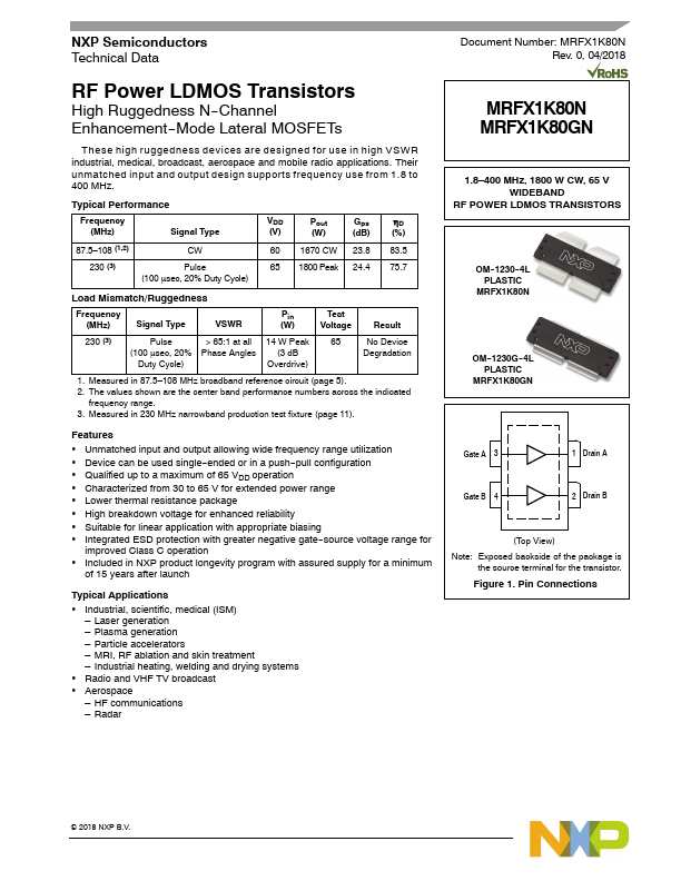
Unmatched input and output allowing wide frequency range utilization Device can be used single--ended or in a push--pull configuration Qualified up to a maximum of 65 VDD operation Characterized from 30 to 65 V for extended power range Lower thermal resistance package High breakdown
voltage for enhanced reliability Suitable for linear application with appropriate biasing Integrated ESD protection with greater negative gate--source
voltage range for
improved Class C operati...