MOTOROLA
SEMICONDUCTOR TECHNICAL DATA
Order this document by MSC3130T1/D
NPN RF Amplifier Transistor Surface Mount
M...
MOTOROLA
SEMICONDUCTOR TECHNICAL DATA
Order this document by MSC3130T1/D
NPN RF Amplifier Transistor Surface Mount
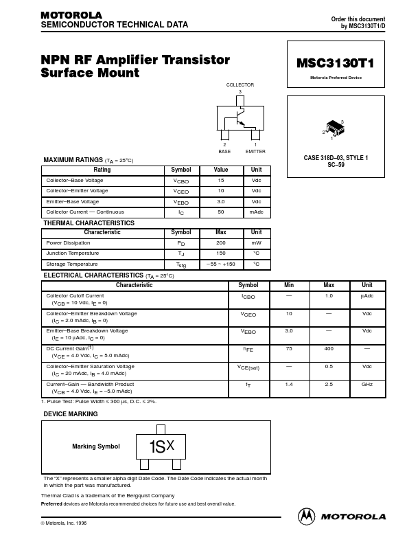
MSC3130T1
Motorola Preferred Device
COLLECTOR 3
3 2 1
2 BASE
1 EMITTER Unit Vdc Vdc Vdc mAdc CASE 318D–03, STYLE 1 SC–59
MAXIMUM RATINGS (TA = 25°C)
Rating Collector–Base
Voltage Collector–Emitter
Voltage Emitter–Base
Voltage Collector Current — Continuous Symbol VCBO VCEO VEBO IC Value 15 10 3.0 50
THERMAL CHARACTERISTICS
Characteristic Power Dissipation Junction Temperature Storage Temperature Symbol PD TJ Tstg Max 200 150 – 55 ~ +150 Unit mW °C °C
ELECTRICAL CHARACTERISTICS (TA = 25°C)
Characteristic Collector Cutoff Current (VCB = 10 Vdc, IE = 0) Collector–Emitter Breakdown
Voltage (IC = 2.0 mAdc, IB = 0) Emitter–Base Breakdown
Voltage (IE = 10 µAdc, IC = 0) DC Current Gain(1) (VCE = 4.0 Vdc, IC = 5.0 mAdc) Collector–Emitter Saturation
Voltage (IC = 20 mAdc, IB = 4.0 mAdc) Current–Gain — Bandwidth Product (VCB = 4.0 Vdc, IE = –5.0 mAdc) 1. Pulse Test: Pulse Width ≤ 300 µs, D.C. ≤ 2%. Symbol ICBO VCEO VEBO hFE VCE(sat) fT Min — 10 3.0 75 — 1.4 Max 1.0 — — 400 0.5 2.5 Unit µAdc Vdc Vdc — Vdc GHz
DEVICE MARKING
Marking Symbol
1SX
The “X” represents a smaller alpha digit Date Code. The Date Code indicates the actual month in which the part was manufactured. Thermal Clad is a trademark of the Bergquist Company
Preferred devices are Motorola recommended choices for future use and best overall value.
© Motorola, Inc. 1996
Motorola Small–Signal Trans...