2 MEG x 16 PAGE FLASH 128K x 16 SRAM COMBO MEMORY
FLASH AND SRAM COMBO MEMORY
FEATURES
• Flexible dual-bank architectur...
2 MEG x 16 PAGE FLASH 128K x 16 SRAM COMBO MEMORY
FLASH AND SRAM COMBO MEMORY
FEATURES
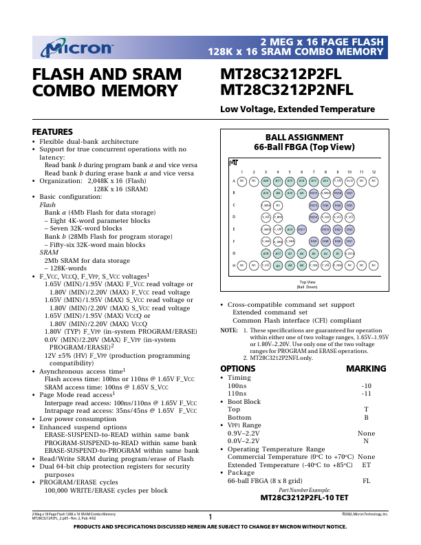
Flexible dual-bank architecture Support for true concurrent operations with no latency: Read bank b during program bank a and vice versa Read bank b during erase bank a and vice versa Organization: 2,048K x 16 (Flash) 128K x 16 (SRAM) Basic configuration: Flash Bank a (4Mb Flash for data storage) – Eight 4K-word parameter blocks – Seven 32K-word blocks Bank b (28Mb Flash for program storage) – Fifty-six 32K-word main blocks SRAM 2Mb SRAM for data storage – 128K-words F_VCC, VCCQ, F_VPP, S_VCC
voltages1 1.65V (MIN)/1.95V (MAX) F_VCC read
voltage or 1.80V (MIN)/2.20V (MAX) F_VCC read
voltage 1.65V (MIN)/1.95V (MAX) S_VCC read
voltage or 1.80V (MIN)/2.20V (MAX) S_VCC read
voltage 1.65V (MIN)/1.95V (MAX) VCCQ or 1.80V (MIN)/2.20V (MAX) VCCQ 1.80V (TYP) F_VPP (in-system PROGRAM/ERASE) 0.0V (MIN)/2.20V (MAX) F_VPP (in-system PROGRAM/ERASE) 2 12V ±5% (HV) F_VPP (production programming compatibility) Asynchronous access time1 Flash access time: 100ns or 110ns @ 1.65V F_VCC SRAM access time: 100ns @ 1.65V S_VCC Page Mode read access1 Interpage read access: 100ns/110ns @ 1.65V F_VCC Intrapage read access: 35ns/45ns @ 1.65V F_VCC Low power consumption Enhanced suspend options ERASE-SUSPEND-to-READ within same bank PROGRAM-SUSPEND-to-READ within same bank ERASE-SUSPEND-to-PROGRAM within same bank Read/Write SRAM during program/erase of Flash Dual 64-bit chip protection registers ...