CYStech Electronics Corp.
20V N-CHANNEL Enhancement Mode MOSFET
MTN2300N3
Spec. No. : C413N3 Issued Date : 2007.07.05 R...
CYStech Electronics Corp.
20V N-CHANNEL Enhancement Mode
MOSFET
MTN2300N3
Spec. No. : C413N3 Issued Date : 2007.07.05 Revised Date : Page No. : 1/5
Features
VDS=20V
RDS(ON)=28mΩ@VGS=4.5V, IDS=6A
RDS(ON)=38mΩ@VGS=2.5V, IDS=5.2A
Low on-resistance Capable of 2.5V gate drive Excellent thermal and electrical capabilities Compact and low profile SOT-23 package
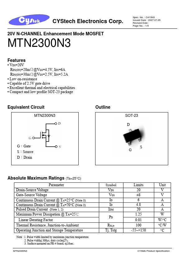
Equivalent Circuit
MTN2300N3
Outline
SOT-23 D
G:Gate S:Source D:Drain
GS
Absolute Maximum Ratings (Ta=25°C)
Parameter Drain-Source
Voltage Gate-Source
Voltage Continuous Drain Current @ TA=25°C (Note 3) Continuous Drain Current @ TA=70°C (Note 3) Pulsed Drain Current (Note 1, 2) Maximum Power Dissipation @ TA=25℃
Linear Derating Factor Thermal Resistance, Junction-to-Ambient Operating Junction and Storage Temperature
Note : 1. Pulse width limited by maximum junction temperature. 2. Pulse width≤ 300μs, duty cycle≤2%. 3. Surface mounted on FR-4 board, t≤10sec.
MTN2300N3
Symbol
VDS VGS ID ID IDM
PD
Rth,ja Tj, Tstg
Limits 20 ±8 6 4.8 20 1.25
0.01
100 -55~+150
Unit V V A A A W
W/°C
°C/W °C
CYStek Product Specification
CYStech Electronics Corp.
Spec. No. : C413N3 Issued Date : 2007.07.05 Revised Date : Page No. : 2/5
Electrical Characteristics (Ta=25°C)
Symbol
Min. Typ. Max. Unit
Test Conditions
Static BVDSS
∆BVDSS/∆Tj VGS(th)
IGSS
IDSS IDSS *RDS(ON)
20 -
- V VGS=0, ID=250μA
- 0.1 - V/°C Reference to 25°C, ID=1mA
0.5 - 1.0 V VDS=VGS, ID=250μA
-
-
±100
nA VGS=±8V, VDS=0
- - 1 μA VDS=20V, VGS=0
...