CYStech Electronics Corp.
30V N-CHANNEL Enhancement Mode MOSFET
Spec. No. : C414N3 Issued Date : 2007.07.05 Revised Dat...
CYStech Electronics Corp.
30V N-CHANNEL Enhancement Mode
MOSFET
Spec. No. : C414N3 Issued Date : 2007.07.05 Revised Date : 2007.12.18 Page No. : 1/ 7
MTN3400N3
Features
VDS=30V RDS(ON)=33mΩ@VGS=4.5V, ID=5A www.DataSheet4U.com RDS(ON)=52mΩ@VGS=2.5V, ID=4A Low on-resistance Low gate charge Excellent thermal and electrical capabilities Compact and low profile SOT-23 package
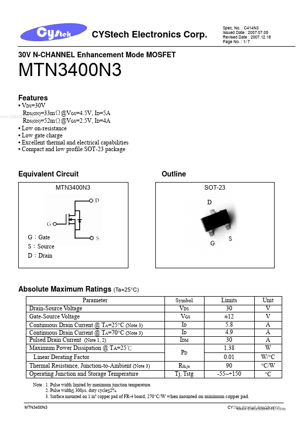
Equivalent Circuit
MTN3400N3
Outline
SOT-23 D
G:Gate S:Source D:Drain
G
S
Absolute Maximum Ratings (Ta=25°C)
Parameter Drain-Source
Voltage Gate-Source
Voltage Continuous Drain Current @ TA=25°C (Note 3) Continuous Drain Current @ TA=70°C (Note 3) Pulsed Drain Current (Note 1, 2) Maximum Power Dissipation @ TA=25℃ Linear Derating Factor Thermal Resistance, Junction-to-Ambient (Note 3) Operating Junction and Storage Temperature
Symbol
VDS VGS ID ID IDM PD Rth,ja Tj, Tstg
Limits 30 ±12 5.8 4.9 30 1.38 0.01 90 -55~+150
Unit V V A A A W W/°C °C/W °C
Note : 1. Pulse width limited by maximum junction temperature. 2. Pulse width≤ 300μs, duty cycle≤2%. 3. Surface mounted on 1 in² copper pad of FR-4 board; 270°C/W when mounted on minimum copper pad.
MTN3400N3 CYStek Product Specification
CYStech Electronics Corp.
Electrical Characteristics (Ta=25°C)
Symbol Static BVDSS VGS(th) GFS IGSS www.DataSheet4U.com IDSS IDSS *RDS(ON) Dynamic Ciss Coss Crss *td(ON) *tr *td(OFF) *tf *Qg *Qgs *Qgd Rg Source-Drain Diode *VSD *IS *trr *Qrr Min. 30 0.7 Typ. 15 823 99 77 3.3 4.8 26.3 4.1 9.7 1.6 3.1 1.2 16 8.9 M...