MOTOROLA
SEMICONDUCTOR TECHNICAL DATA
Order this document by MTP12N06EZL/D
™ Data Sheet TMOS E-FET.™ High Energy Powe...
MOTOROLA
SEMICONDUCTOR TECHNICAL DATA
Order this document by MTP12N06EZL/D
™ Data Sheet TMOS E-FET.™ High Energy Power FET
Designer's
MTP12N06EZL
N–Channel Enhancement–Mode Silicon Gate
This advanced TMOS power FET is designed to withstand high energy in the avalanche mode and switch efficiently. This new high energy device also offers a gate–to–source zener diode designed for 4 kV ESD protection (human body model). ESD Protected 4 kV Human Body Model 400 V Machine Model Avalanche Energy Capability Internal Source–To–Drain Diode Designed to Replace External Zener Transient Suppressor–Absorbs High Energy in the Avalanche Mode
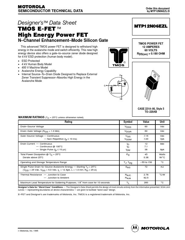
G
TMOS POWER FET 12 AMPERES 60 VOLTS RDS(on) = 0.180 OHM
®
D
S
CASE 221A–06, Style 5 TO–220AB
MAXIMUM RATINGS (TC = 25°C unless otherwise noted)
Rating Drain–Source
Voltage Drain–Gate
Voltage (RGS = 1.0 MΩ) Gate–Source
Voltage — Continuous Gate–Source
Voltage — Non–Repetitive (tp ≤ 10 ms) Drain Current — Continuous — Continuous @ 100°C — Single Pulse (tp ≤ 10 µs) Total Power Dissipation @ TC = 25°C Derate above 25°C Operating and Storage Temperature Range Single Pulse Drain–to–Source Avalanche Energy — Starting TJ = 25°C (VDD = 25 Vdc, VGS = 5.0 Vdc, IL = 12 Apk, L = 1.0 mH, RG = 25 Ω) Thermal Resistance — Junction to Case — Junction to Ambient Maximum Lead Temperature for Soldering Purposes, 1/8″ from case for 10 seconds Symbol VDSS VDGR VGS VGSM ID ID IDM PD TJ, Tstg EAS RθJC RθJA TL Value 60 60 ± 15 ± 20 12 7.1 36 45 0.36 – 55 to 1...