MTP3055VL
June 2000 DISTRIBUTION GROUP*
MTP3055VL
N-Channel Logic Level Enhancement Mode Field Effect Transistor
Gene...
MTP3055VL
June 2000 DISTRIBUTION GROUP*
MTP3055VL
N-Channel Logic Level Enhancement Mode Field Effect Transistor
General Description
This N-Channel Logic Level
MOSFET has been designed specifically for low
voltage, high speed switching applications i.e. power supplies and power motor controls.
This
MOSFET features faster switching and lower gate charge than other
MOSFETs with comparable RDS(ON) specifications.
The result is a
MOSFET that is easy and safer to drive (even at very high frequencies).
Features
12 A, 60 V. RDS(ON) = 0.18 Ω @ VGS = 5 V
Critical DC electrical parameters specified at elevated temperature.
Low drive requirements allowing operation directly from logic drivers. Vgs(th) < 2 V.
Rugged internal source-drain diode can eliminate the need for an external Zener diode transient suppressor.
175°C maximum junction temperature rating.
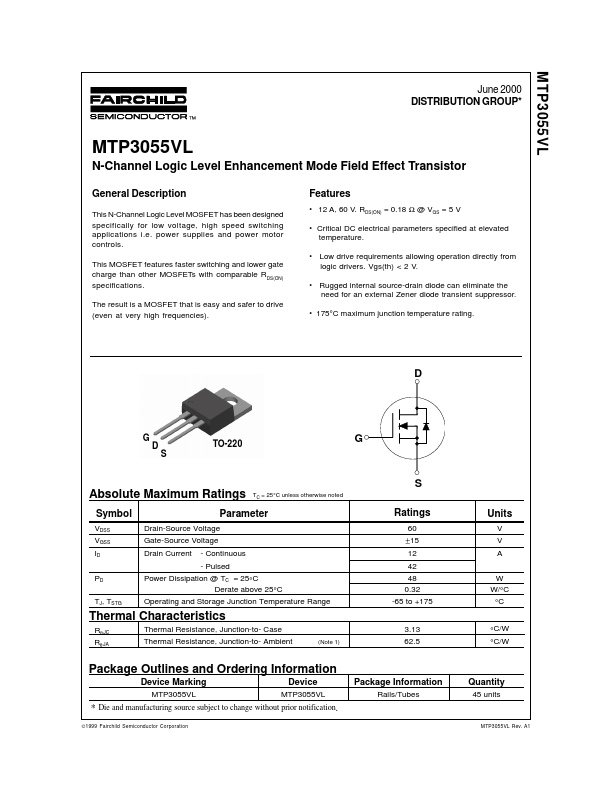
D
G D S
TO-220
G
Absolute Maximum Ratings TC = 25°C unless otherwise noted
Symbol
Parameter
VDSS
Drain-Source
Voltage
VGSS
Gate-Source
Voltage
ID Drain Current - Continuous
- Pulsed
PD TJ, TSTG
Power Dissipation @ TC = 25°C Derate above 25°C
Operating and Storage Junction Temperature Range
Thermal Characteristics
RθJC Thermal Resistance, Junction-to- Case
Rθ JA
Thermal Resistance, Junction-to- Ambient
(Note 1)
S
Ratings
60 ±15 12 42 48 0.32 -65 to +175
3.13 62.5
Package Outlines and Ordering Information
Device Marking
Device
MTP3055VL
MTP3055VL
* Die and manufacturing source subject to change w...