MOTOROLA
SEMICONDUCTOR TECHNICAL DATA
Order this document by MTV20N50E/D
™ Data Sheet TMOS E-FET.™ Power Field Effect...
MOTOROLA
SEMICONDUCTOR TECHNICAL DATA
Order this document by MTV20N50E/D
™ Data Sheet TMOS E-FET.™ Power Field Effect Transistor D3PAK for Surface Mount
Designer's
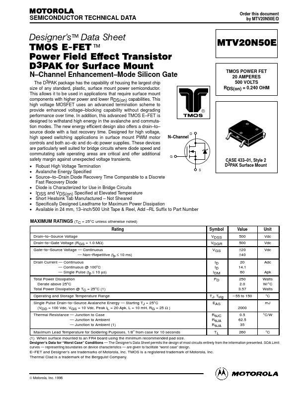
MTV20N50E
TMOS POWER FET 20 AMPERES 500 VOLTS RDS(on) = 0.240 OHM
N–Channel Enhancement–Mode Silicon Gate
The D3PAK package has the capability of housing the largest chip size of any standard, plastic, surface mount power semiconductor. This allows it to be used in applications that require surface mount components with higher power and lower RDS(on) capabilities. This high
voltage MOSFET uses an advanced termination scheme to provide enhanced
voltage–blocking capability without degrading performance over time. In addition, this advanced TMOS E–FET is designed to withstand high energy in the avalanche and commutation modes. The new energy efficient design also offers a drain–to– source diode with a fast recovery time. Designed for high
voltage, high speed switching applications in surface mount PWM motor controls and both ac–dc and dc–dc power supplies. These devices are particularly well suited for bridge circuits where diode speed and commutating safe operating areas are critical and offer additional safety margin against unexpected
voltage transients.
®
D N–Channel
G CASE 433–01, Style 2 D3PAK Surface Mount
Robust High
Voltage Termination S Avalanche Energy Specified Source–to–Drain Diode Recovery Time Comparable to a Discrete Fast Recovery Diode Diode is Characterized for Use in Bridge Circuits...