MUN5116DW1, NSBA143TDXV6
Dual PNP Bias Resistor Transistors R1 = 4.7 kW, R2 = 8 kW
PNP Transistors with Monolithic Bias...
MUN5116DW1, NSBA143TDXV6
Dual PNP Bias Resistor Transistors R1 = 4.7 kW, R2 = 8 kW
PNP Transistors with Monolithic Bias Resistor Network
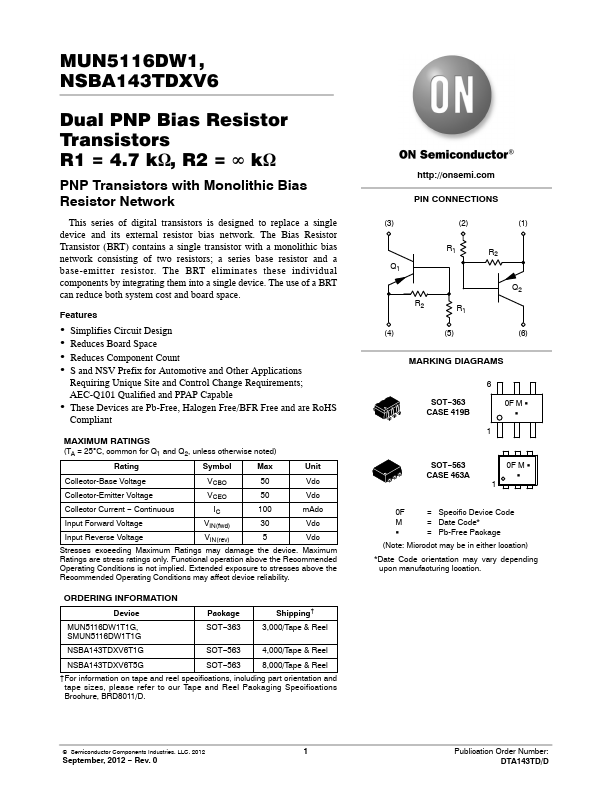
This series of digital transistors is designed to replace a single device and its external resistor bias network. The Bias Resistor Transistor (BRT) contains a single transistor with a monolithic bias network consisting of two resistors; a series base resistor and a base-emitter resistor. The BRT eliminates these individual components by integrating them into a single device. The use of a BRT can reduce both system cost and board space.
Features
Simplifies Circuit Design Reduces Board Space Reduces Component Count S and NSV Prefix for Automotive and Other Applications
Requiring Unique Site and Control Change Requirements; AEC-Q101 Qualified and PPAP Capable
These Devices are Pb-Free, Halogen Free/BFR Free and are RoHS
Compliant
MAXIMUM RATINGS (TA = 25C, common for Q1 and Q2, unless otherwise noted)
Rating
Symbol
Max
Unit
Collector-Base
Voltage
VCBO
50
Vdc
Collector-Emitter
Voltage
VCEO
50
Vdc
Collector Current − Continuous IC 100 mAdc
Input Forward
Voltage
VIN(fwd)
30
Vdc
Input Reverse
Voltage
VIN(rev)
5
Vdc
Stresses exceeding Maximum Ratings may damage the device. Maximum Ratings are stress ratings only. Functional operation above the Recommended Operating Conditions is not implied. Extended exposure to stresses above the Recommended Operating Conditions may affect device reliability.
ORDERING INFORMAT...