TinyLogic ULP-A Triple Buffer
NC7NP34
The NC7NP34 is a triple buffer in tiny footprint packages. The device is designed...
TinyLogic ULP-A Triple Buffer
NC7NP34
The NC7NP34 is a triple buffer in tiny footprint packages. The device is designed to operate for VCC = 0.9 V to 3.6 V.
Features
Designed for 0.9 V to 3.6 V VCC Operation 2.7 ns tPD at 3.3 V (Typ) Inputs/Outputs Over−
Voltage Tolerant up to 3.6 V IOFF Supports Partial Power Down Protection Source/Sink 2.6 mA at 3.3 V Available in US8 and MicroPak™ Packages These Devices are Pb−Free, Halogen Free/BFR Free and are RoHS
Compliant
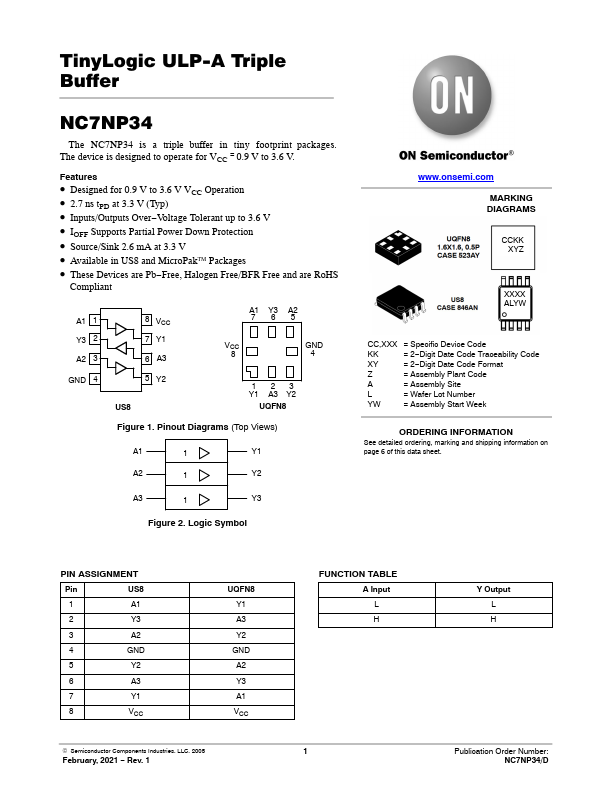
A1 1 Y3 2 A2 3 GND 4
8 VCC 7 Y1 6 A3
A1 Y3 A2 765
VCC
GND
8
4
5 Y2 US8
123 Y1 A3 Y2
UQFN8
Figure 1. Pinout Diagrams (Top Views)
A1
1
Y1
A2
1
Y2
A3
1
Y3
Figure 2. Logic Symbol
www.onsemi.com MARKING DIAGRAMS
CCKK XYZ
XXXX ALYW
CC,XXX = Specific Device Code
KK
= 2−Digit Date Code Traceability Code
XY
= 2−Digit Date Code Format
Z
= Assembly Plant Code
A
= Assembly Site
L
= Wafer Lot Number
YW
= Assembly Start Week
ORDERING INFORMATION
See detailed ordering, marking and shipping information on page 6 of this data sheet.
PIN ASSIGNMENT
Pin
US8
1
A1
2
Y3
3
A2
4
GND
5
Y2
6
A3
7
Y1
8
VCC
UQFN8 Y1 A3 Y2
GND A2 Y3 A1 VCC
© Semiconductor Components Industries, LLC, 2005
February, 2021 − Rev. 1
FUNCTION TABLE A Input L H
1
Y Output L H
Publication Order Number: NC7NP34/D
NC7NP34
MAXIMUM RATINGS
Symbol
Characteristics
Value
Unit
VCC VIN VOUT
IIK IOK IOUT ICC or IGND TSTG TL TJ qJA
DC Supply
Voltage
DC Input
Voltage
DC Output
Voltage
DC Input Diode ...