NCP511, NCV511
Voltage Regulator - CMOS, Low Iq, Low-Dropout
150 mA
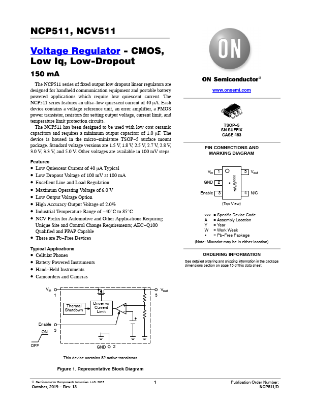
The NCP511 series of fixed output low dropout linear regulators are designed for handheld communication equipment and portable battery powered applications which require low quiescent current. The NCP511 series features an ultra−low quiescent current of 40 mA. Each device contains a voltag...