ND2012L/2020L
N-Channel Depletion-Mode MOSFET Transistors
Product Summary
Part Number
ND2012L ND2020L
V(BR)DSV Min (V)
...
ND2012L/2020L
N-Channel Depletion-Mode
MOSFET Transistors
Product Summary
Part Number
ND2012L ND2020L
V(BR)DSV Min (V)
200
rDS(on) Max (W)
12 20
VGS(off) (V)
–1.5 to –4 –0.5 to –2.5
ID (A)
0.16 0.132
Features
D D D D D High Breakdown
Voltage: 220 V Normally “On” Low rDS Switch: 9 W Low Input and Output Leakage Low-Power Drive Requirement Low Input Capacitance
Benefits
D D D D D Full-
Voltage Operation Low Offset
Voltage Low Error
Voltage Easily Driven Without Buffer High-Speed Switching
Applications
D D D D D Normally “On” Switching Circuits Current Sources/Limiters Power Supply, Converter Circuits Solid-State Relays Telecom Switches
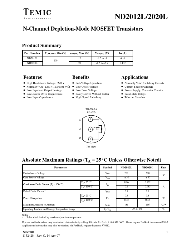
TO-226AA (TO-92) S 1
G
2
D
3 Top View
Absolute Maximum Ratings (TA = 25_C Unless Otherwise Noted)
Parameter
Drain-Source
Voltage Gate-Source
Voltage Continuous Drain Current (TJ = 150_C) Pulsed Drain Currenta TA= 25_C TA= 100_C TA= 25_C TA= 100_C
Symbol
VDS VGS ID IDM PD RthJA TJ, Tstg
ND2012L
200 "30 0.16 0.1 0.8 0.8 0.32 156
ND2020L
200 "30 0.132 0.083 0.8 0.8 0.32 156
Unit
V
A
Power Dissipation Maximum Junction-to-Ambient Operating Junction and Storage Temperature Range
W _C/W _C
–55 to 150
Notes a. Pulse width limited by maximum junction temperature. Updates to this data sheet may be obtained via facsimile by calling Siliconix FaxBack, 1-408-970-5600. Please request FaxBack document #70197. Applications information may also be obtained via FaxBack, request document #70612.
Siliconix S-52426—Rev. C, 14-Apr-97
1
ND2012L/...