November 1996
NDP6020 / NDB6020 N-Channel Logic Level Enhancement Mode Field Effect Transistor
General Description
Thes...
November 1996
NDP6020 / NDB6020 N-Channel Logic Level Enhancement Mode Field Effect Transistor
General Description
These logic level N-Channel enhancement mode power field effect transistors are produced using National's proprietary, high cell density, DMOS technology. This very high density process has been especially tailored to minimize on-state resistance, provide superior switching performance, and withstand high energy pulses in the avalanche and commutation modes. These devices are particularly suited for low
voltage applications such as automotive, DC/DC converters, PWM motor controls, and other battery powered circuits where fast switching, low in-line power loss, and resistance to transients are needed.
Features
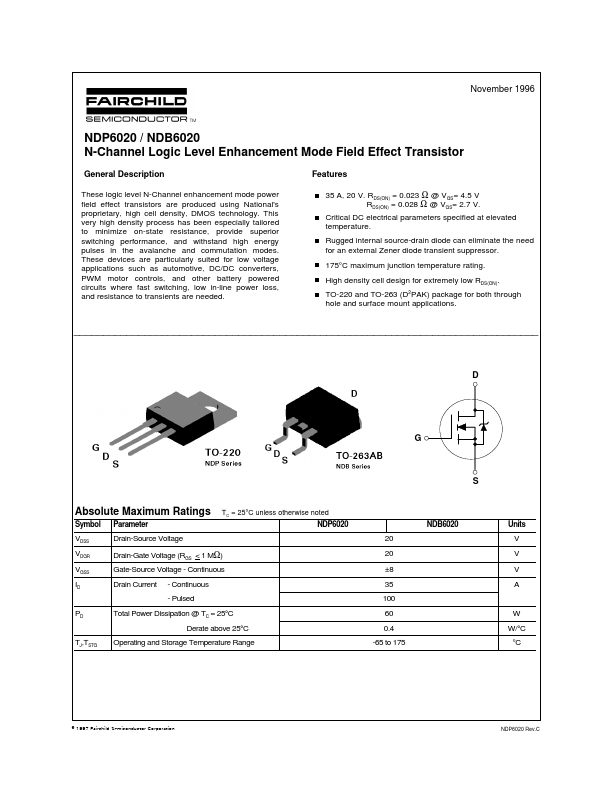
35 A, 20 V. RDS(ON) = 0.023 Ω @ VGS= 4.5 V RDS(ON) = 0.028 Ω @ VGS= 2.7 V. Critical DC electrical parameters specified at elevated temperature. Rugged internal source-drain diode can eliminate the need for an external Zener diode transient suppressor. 175°C maximum junction temperature rating. High density cell design for extremely low RDS(ON). TO-220 and TO-263 (D2PAK) package for both through hole and surface mount applications.
_______________________________________________________________________________
D
G
S
Absolute Maximum Ratings
Symbol Parameter
TC = 25°C unless otherwise noted
NDP6020
NDB6020
Units
VDSS VDGR VGSS ID
Drain-Source
Voltage Drain-Gate
Voltage (RGS < 1 MΩ) Gate-Source
Voltage - Continuous Drain Current - Continuous - Puls...