www.DataSheet4U.com
NEC's NPN SILICON TRANSISTOR NE685M13
FEATURES
• NEW MINIATURE M13 PACKAGE: – Small transistor out...
www.DataSheet4U.com
NEC's NPN SILICON TRANSISTOR NE685M13
FEATURES
NEW MINIATURE M13 PACKAGE: – Small transistor outline – 1.0 X 0.5 X 0.5 mm – Low profile / 0.50 mm package height – Flat lead style for better RF performance HIGH GAIN BANDWIDTH PRODUCT: fT = 12 GHz
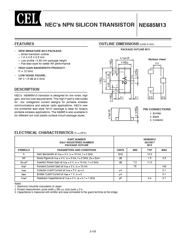
OUTLINE DIMENSIONS (Units in mm)
PACKAGE OUTLINE M13
0.15+0.1 ñ0.05
0.7±0.05 0.5+0.1 ñ0.05
0.2+0.1 ñ0.05
(Bottom View)
0.3
0.35
1.0+0.1 ñ0.05
0.7
LOW NOISE FIGURE: NF = 1.5 dB at 2 GHz
2
3
Y2
0.35
1
DESCRIPTION
NEC's NE685M13 transistor is designed for low noise, high gain, and low cost requirements. This high fT part is well suited for low
voltage/low current designs for portable wireless communications and cellular radio applications. NEC's new low profile/flat lead style "M13" package is ideal for today's portable wireless applications. The NE685 is also available in six different low cost plastic surface mount package styles.
0.15+0.1 ñ0.05
0.1
0.1
0.2
0.2
0.125+0.1 ñ0.05
0.5±0.05
PIN CONNECTIONS
1. Emitter 2. Base 3. Collector
ELECTRICAL CHARACTERISTICS (TA = 25°C)
PART NUMBER EIAJ1 REGISTERED NUMBER PACKAGE OUTLINE SYMBOLS fT NF |S21E|2 hFE2 ICBO IEBO CRE3 PARAMETERS AND CONDITIONS Gain Bandwidth at VCE = 3 V, IC = 10 mA, f = 2 GHz Noise Figure at VCE = 3 V, IC = 3 mA, f = 2 GHz, ZS = ZOPT Insertion Power Gain at VCE = 3 V, IC = 10 mA, f = 2 GHz Forward Current Gain at VCE = 3 V, IC = 10 mA Collector Cutoff Current at VCB = 5 V, IE = 0 Emitter Cutoff Current at VEB = 1 V, IC = 0...