Preliminary Data Sheet
NP89N04MUK, NP89N04NUK
MOS FIELD EFFECT TRANSISTOR
R07DS0599EJ0100 Rev.1.00
Jan 11, 2012
Descr...
Preliminary Data Sheet
NP89N04MUK, NP89N04NUK
MOS FIELD EFFECT TRANSISTOR
R07DS0599EJ0100 Rev.1.00
Jan 11, 2012
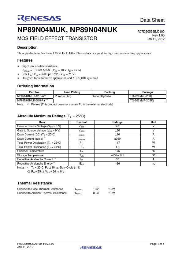
Description
These products are N-channel MOS Field Effect Transistors designed for high current switching applications.
Features
Super low on-state resistance RDS(on) = 3.3 m MAX. (VGS = 10 V, ID = 45 A)
Low Ciss: Ciss = 3900 pF TYP. (VDS = 25 V) Designed for automotive application and AEC-Q101 qualified
Ordering Information
Part No. NP89N04MUK-S18-AY *1 NP89N04NUK-S18-AY *1
Lead Plating Pure Sn (Tin)
Packing Tube 50 p/tube
Note: *1 Pb-free (This product does not contain Pb in the external electrode)
Package TO-220 (MP-25K) TO-262 (MP-25SK)
Absolute Maximum Ratings (TA = 25°C)
Item
Symbol
Drain to Source
Voltage (VGS = 0 V)
VDSS
Gate to Source
Voltage (VDS = 0 V)
VGSS
Drain Current (DC) (TC = 25°C) Drain Current (pulse) *1
ID(DC) ID(pulse)
Total Power Dissipation (TC = 25°C)
PT1
Total Power Dissipation (TA = 25°C)
PT2
Channel Temperature
Tch
Storage Temperature Repetitive Avalanche Current *2 Repetitive Avalanche Energy *2
Tstg IAR EAR
Notes: *1 TC = 25°C, PW 10 s, Duty Cycle 1% *2 RG = 25 , VGS = 20 0 V
Ratings 40 20 90
360 147 1.8 175 –55 to 175 37 136
Unit V V A A W W °C °C A mJ
Thermal Resistance
Channel to Case Thermal Resistance Channel to Ambient Thermal Resistance
Rth(ch-C) Rth(ch-A)
1.02 °C/W 83.3 °C/W
R07DS0599EJ0100 Rev.1.00 Jan 11, 2012
Page 1 of 6
NP89N04MUK, NP89N04NUK
Electrical Characteristics (TA...