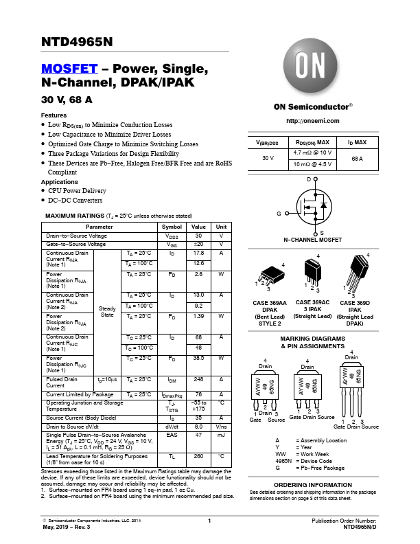
NTD4965N
MOSFET – Power, Single, N-Channel, DPAK/IPAK
30 V, 68 A
Features
• Low RDS(on) to Minimize Conduction Losses...
NTD4965N
MOSFET – Power, Single, N-Channel, DPAK/IPAK
30 V, 68 A
Features
Low RDS(on) to Minimize Conduction Losses Low Capacitance to Minimize Driver Losses Optimized Gate Charge to Minimize Switching Losses Three Package Variations for Design Flexibility These Devices are Pb−Free, Halogen Free/BFR Free and are RoHS
Compliant
Applications
CPU Power Delivery DC−DC Converters
MAXIMUM RATINGS (TJ = 25°C unless otherwise stated)
Parameter
Symbol Value Unit
Drain−to−Source
Voltage
Gate−to−Source
Voltage
Continuous Drain Current RqJA (Note 1)
VDSS
30
V
VGS
±20
V
TA = 25°C
ID
17.8
A
TA = 100°C
12.6
Power Dissipation RqJA (Note 1)
TA = 25°C
PD
2.6
W
Continuous Drain
TA = 25°C
ID
Current RqJA (Note 2)
Steady TA = 100°C
Power
State
TA = 25°C
PD
Dissipation RqJA
(Note 2)
13.0
A
9.2
1.39
W
Continuous Drain Current RqJC (Note 1)
TC = 25°C
ID
TC = 100°C
68
A
48
Power Dissipation RqJC (Note 1)
TC = 25°C
PD
38.5
W
Pulsed Drain Current
tp=10ms TA = 25°C
IDM
248
A
Current Limited by Package TA = 25°C Operating Junction and Storage Temperature
Source Current (Body Diode)
Drain to Source dV/dt
Single Pulse Drain−to−Source Avalanche Energy (TJ = 25°C, VDD = 24 V, VGS = 10 V, IL = 31 Apk, L = 0.1 mH, RG = 25 W) Lead Temperature for Soldering Purposes (1/8” from case for 10 s)
IDmaxPkg TJ, TSTG IS
dV/dt EAS
TL
76 −55 to +175
35 6.0 47
260
A °C
A V/ns mJ
°C
Stresses exceeding those listed in the Maximum Ratings table may da...