NTHD5905T1
Power MOSFET Dual P−Channel ChipFETt
3.0 Amps, 8 Volts
Features
• Low RDS(on) for Higher Efficiency • Logic ...
NTHD5905T1
Power
MOSFET Dual P−Channel ChipFETt
3.0 Amps, 8 Volts
Features
Low RDS(on) for Higher Efficiency Logic Level Gate Drive Miniature ChipFET Surface Mount Package
Applications
Power Management in Portable and Battery−Powered Products; i.e.,
Cellular and Cordless Telephones and PCMCIA Cards
http://onsemi.com
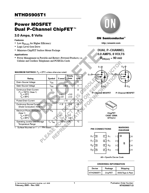
DUAL P−CHANNEL 3.0 AMPS, 8 VOLTS
RDS(on) = 90 mW
MAXIMUM RATINGS (TA = 25°C unless otherwise noted)
Rating
Steady Symbol 5 secs State
Drain−Source
Voltage
Gate−Source
Voltage
Continuous Drain Current (TJ = 150°C) (Note 1) TA = 25°C TA = 85°C
Pulsed Drain Current
Continuous Source Current (Diode Conduction) (Note 1)
VDS −8.0 VGS "8.0 ID
"4.1 "2.9
"3.0 "2.2
IDM "10
IS −1.8 −0.9
Maximum Power Dissipation (Note 1) TA = 25°C TA = 85°C
Operating Junction and Storage Temperature Range
PD TJ, Tstg
2.1 1.1 1.1 0.6
−55 to +150
1. Surface Mounted on 1″ x 1″ FR4 Board.
Unit V V A
A A W
°C
S1 G1
S2 G2
D1 P−Channel
MOSFET
D2 P−Channel
MOSFET
ChipFET CASE 1206A
STYLE 2
PIN CONNECTIONS
MARKING DIAGRAM
D1 8 D1 7 D2 6 D2 5
1 S1 2 G1 3 S2 4 G2
1 2 3 4
A9
8 7 6 5
A9 = Specific Device Code
ORDERING INFORMATION
Device
Package
Shipping
NTHD5905T1 ChipFET
3000/Tape & Reel
© Semiconductor Components Industries, LLC, 2005
February, 2005 − Rev. XXX
1
Publication Order Number: NTHD5905T1/D
NTHD5905T1
THERMAL CHARACTERISTICS
Characteristic
Symbol
Typ
Maximum Junction−to−Ambient (Note 2) t v 5 sec Steady State
RthJA
50 90
Maximum Junction−...