MOSFET - Power, Single N-Channel, WDFN6
20 V
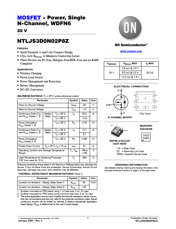
NTLJS3D0N02P8Z
Features
• Small Footprint (4 mm2) for Compact Design • Ul...
MOSFET - Power, Single N-Channel, WDFN6
20 V
NTLJS3D0N02P8Z
Features
Small Footprint (4 mm2) for Compact Design Ultra−Low RDS(on) to Minimize Conduction Losses These Devices are Pb−Free, Halogen−Free/BFR−Free and are RoHS
Compliant
Applications
Wireless Charging Power Load Switch Power Management and Protection Battery Management DC−DC Converters
MAXIMUM RATINGS (TJ = 25°C unless otherwise noted)
Parameter
Symbol Value Unit
Drain−to−Source
Voltage
VDSS
20
V
Gate−to−Source
Voltage
VGS
±12
V
Continuous Drain Cur- Steady TA = 25°C
ID
20.2 A
rent RqJA (Notes 1, 3) State
TA = 85°C
14.6
Power Dissipation RqJA (Notes 1, 3)
TA = 25°C
PD
2.40 W
Continuous Drain Cur- Steady TA = 25°C
ID
12.1 A
rent RqJA (Notes 2, 3) State
TA = 85°C
8.7
Power Dissipation RqJA (Notes 2, 3)
TA = 25°C
PD
0.86 W
Pulsed Drain Current TA = 25°C, tp = 10 ms
IDM
81
A
Operating Junction and Storage Temperature Range
TJ, Tstg −55 to °C +150
Lead Temperature for Soldering Purposes (1/8″ from case for 10 s)
TL
260 °C
Stresses exceeding those listed in the Maximum Ratings table may damage the device. If any of these limits are exceeded, device functionality should not be assumed, damage may occur and reliability may be affected.
THERMAL RESISTANCE MAXIMUM RATINGS (Note 1)
Parameter
Symbol Value Unit
Junction−to−Ambient − Steady State (Note 1)
RqJA
52 °C/W
Junction−to−Ambient − Steady State (Note 2)
RqJA
145
1. Surface−mounted on FR4 board using 1 in...