MOSFET - N-Channel Shielded Gate PowerTrench[
150 V, 7.3 mW, 101 A
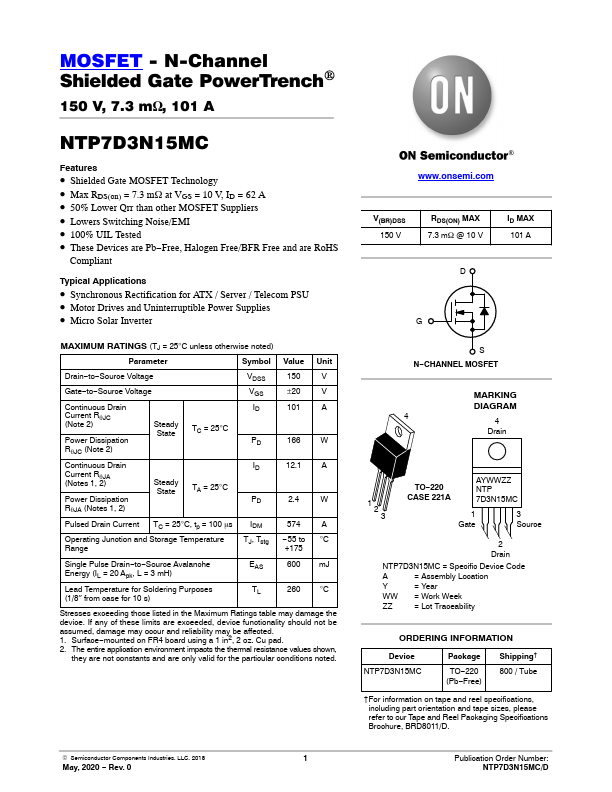
NTP7D3N15MC
Features
• Shielded Gate MOSFET Technol...
MOSFET - N-Channel Shielded Gate PowerTrench[
150 V, 7.3 mW, 101 A
NTP7D3N15MC
Features
Shielded Gate
MOSFET Technology Max RDS(on) = 7.3 mW at VGS = 10 V, ID = 62 A 50% Lower Qrr than other
MOSFET Suppliers Lowers Switching Noise/EMI 100% UIL Tested These Devices are Pb−Free, Halogen Free/BFR Free and are RoHS
Compliant
Typical Applications
Synchronous Rectification for ATX / Server / Telecom PSU Motor Drives and Uninterruptible Power Supplies Micro Solar Inverter
MAXIMUM RATINGS (TJ = 25°C unless otherwise noted)
Parameter
Symbol Value Unit
Drain−to−Source
Voltage
VDSS
150
V
Gate−to−Source
Voltage
VGS
±20
V
Continuous Drain Current RqJC (Note 2)
Power Dissipation RqJC (Note 2)
ID
Steady State
TC = 25°C
PD
101
A
166 W
Continuous Drain Current RqJA (Notes 1, 2)
Power Dissipation RqJA (Notes 1, 2)
ID
Steady State
TA = 25°C
PD
12.1 A
2.4
W
Pulsed Drain Current TC = 25°C, tp = 100 ms IDM
574
A
Operating Junction and Storage Temperature Range
TJ, Tstg − 55 to °C +175
Single Pulse Drain−to−Source Avalanche Energy (IL = 20 Apk, L = 3 mH)
Lead Temperature for Soldering Purposes (1/8″ from case for 10 s)
EAS
600 mJ
TL
260 °C
Stresses exceeding those listed in the Maximum Ratings table may damage the device. If any of these limits are exceeded, device functionality should not be assumed, damage may occur and reliability may be affected. 1. Surface−mounted on FR4 board using a 1 in2, 2 oz. Cu pad. 2. The entire application envir...