NTR0202PL Power MOSFET
−20 V, −400 mA, P−Channel SOT−23 Package
Features
• Low RDS(on) Provides Higher Efficiency and E...
NTR0202PL Power
MOSFET
−20 V, −400 mA, P−Channel SOT−23 Package
Features
Low RDS(on) Provides Higher Efficiency and Extends Battery Life
RDSon = 0.80 W, VGS = −10 V RDSon = 1.10 W, VGS = −4.5 V Miniature SOT−23 Surface Mount Package Saves Board Space Pb−Free Package is Available
V(BR)DSS −20 V
http://onsemi.com
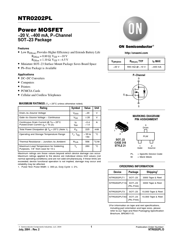
RDS(on) TYP 550 mW @ −10 V P−Channel D ID MAX −400 mA
Applications
DC−DC Converters Computers Printers PCMCIA Cards Cellular and Cordless Telephones
G
MAXIMUM RATINGS (TJ = 25°C unless otherwise noted)
Rating Drain−to−Source
Voltage Gate−to−Source
Voltage − Continuous Continuous Drain Current @ TA = 25°C Pulsed Drain Current (tp ≤ 10 ms) Total Power Dissipation @ TA = 25°C (Note 1) Operating and Storage Temperature Range Thermal Resistance − Junction−to−Ambient Maximum Lead Temperature for Soldering Purposes, 1/8″ from case for 10 s Symbol VDSS VGS ID IDM PD TJ, Tstg RqJA TL Value −20 $20 −0.4 −1.0 225 − 55 to 150 556 260 Unit V V A mW °C °C/W °C 3
S
MARKING DIAGRAM/ PIN ASSIGNMENT
3 Drain 1 2 SOT−23 CASE 318 STYLE 21 PLW
1 Gate PL W
2 Source
Maximum ratings are those values beyond which device damage can occur. Maximum ratings applied to the device are individual stress limit values (not normal operating conditions) and are not valid simultaneously. If these limits are exceeded, device functional operation is not implied, damage may occur and reliability may be affected. 1. Pulse Test: Pulse Width v 300 ms, Duty Cycle v 2%.
= Specific Devic...