NTR5103N
MOSFET – Single, N-Channel, Small Signal, SOT-23
60 V, 310 mA
Features
• Low RDS(on) • Small Footprint Surfac...
NTR5103N
MOSFET – Single, N-Channel, Small Signal, SOT-23
60 V, 310 mA
Features
Low RDS(on) Small Footprint Surface Mount Package Trench Technology These Devices are Pb−Free, Halogen Free/BFR Free and are RoHS
Compliant
Applications
Low Side Load Switch Level Shift Circuits DC−DC Converter Portable Applications i.e. DSC, PDA, Cell Phone, etc.
MAXIMUM RATINGS (TJ = 25°C unless otherwise stated)
Rating
Symbol Value
Unit
Drain−to−Source
Voltage Gate−to−Source
Voltage Drain Current (Note 1)
Steady State
VDSS
60
V
VGS ±30
V
TA = 25°C TA = 85°C
ID
mA 260 190
t<5s Power Dissipation (Note 1)
Steady State t<5s
TA = 25°C TA = 85°C
PD
310 220
mW 300 420
Pulsed Drain Current (tp = 10 ms) Operating Junction and Storage Temperature Range
IDM TJ, TSTG
1.2 −55 to +150
A °C
Source Current (Body Diode)
IS 300 mA
Lead Temperature for Soldering Purposes TL 260 °C (1/8″ from case for 10 s)
Stresses exceeding those listed in the Maximum Ratings table may damage the device. If any of these limits are exceeded, device functionality should not be assumed, damage may occur and reliability may be affected. THERMAL CHARACTERISTICS
Characteristic
Symbol Max
Unit
Junction−to−Ambient − Steady State (Note 1)
RqJA
417 °C/W
Junction−to−Ambient − t ≤ 5 s (Note 1)
RqJA
300
1. Surface−mounted on FR4 board using 1 in sq pad size (Cu area = 1.127 in sq [1 oz] including traces)
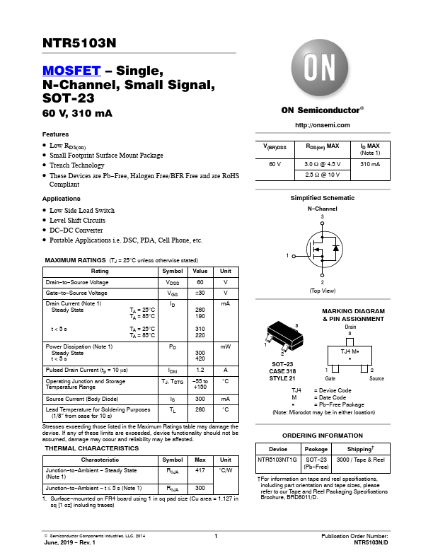
http://onsemi.com
V(BR)DSS 60 V
RDS(on) MAX
3.0 W @ 4.5 V 2.5 W @ 10 V
ID MAX (Not...