NTGS3130N, NVGS3130N
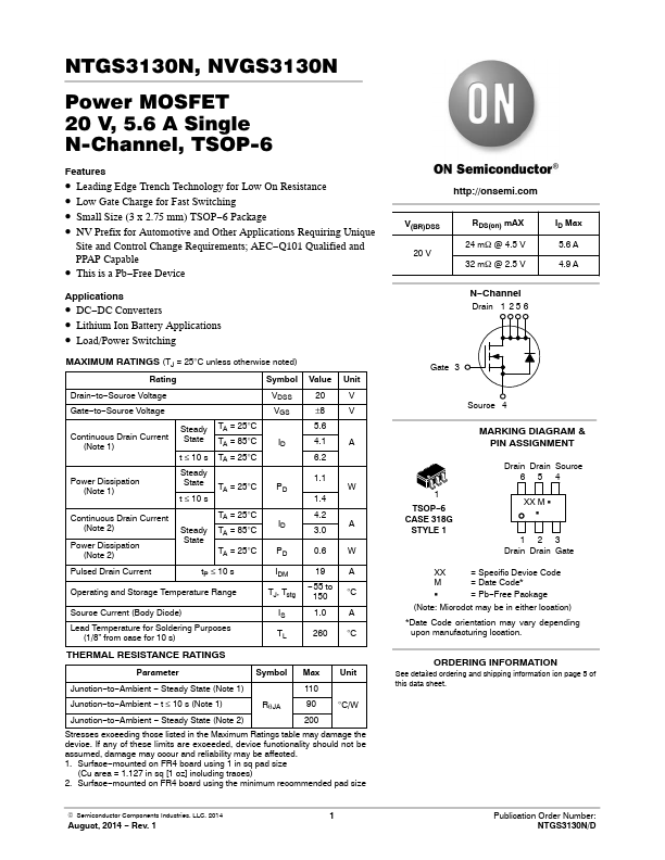
Power MOSFET 20 V, 5.6 A Single N-Channel, TSOP-6
Features
• Leading Edge Trench Technology for L...
NTGS3130N, NVGS3130N
Power
MOSFET 20 V, 5.6 A Single N-Channel, TSOP-6
Features
Leading Edge Trench Technology for Low On Resistance
Low Gate Charge for Fast Switching
Small Size (3 x 2.75 mm) TSOP−6 Package
NV Prefix for Automotive and Other Applications Requiring Unique
Site and Control Change Requirements; AEC−Q101 Qualified and PPAP Capable
This is a Pb−Free Device
Applications
DC−DC Converters Lithium Ion Battery Applications Load/Power Switching
MAXIMUM RATINGS (TJ = 25°C unless otherwise noted)
Rating
Symbol Value Unit
Drain−to−Source
Voltage Gate−to−Source
Voltage
VDSS 20 V VGS ±8 V
Continuous Drain Current (Note 1)
Power Dissipation (Note 1)
Steady State
t ≤ 10 s Steady State t ≤ 10 s
TA = 25°C TA = 85°C TA = 25°C
TA = 25°C
ID PD
5.6 4.1 A 6.2
1.1 W
1.4
Continuous Drain Current (Note 2)
Power Dissipation (Note 2)
Steady State
TA = 25°C TA = 85°C
TA = 25°C
ID PD
4.2 3.0 A 0.6 W
Pulsed Drain Current
tP ≤ 10 s
Operating and Storage Temperature Range
IDM TJ, Tstg
19 −55 to
150
A °C
Source Current (Body Diode) Lead Temperature for Soldering Purposes
(1/8” from case for 10 s)
IS 1.0 A TL 260 °C
THERMAL RESISTANCE RATINGS
Parameter
Symbol Max Unit
Junction−to−Ambient − Steady State (Note 1)
110
Junction−to−Ambient − t ≤ 10 s (Note 1) Junction−to−Ambient − Steady State (Note 2)
RqJA
90 °C/W 200
Stresses exceeding those listed in the Maximum Ratings table may damage the device. If any of these limits are exceeded, device func...