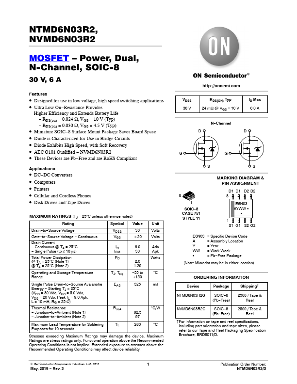
NTMD6N03R2, NVMD6N03R2
MOSFET – Power, Dual, N-Channel, SOIC-8
30 V, 6 A
Features
• Designed for use in low voltage, h...
NTMD6N03R2, NVMD6N03R2
MOSFET – Power, Dual, N-Channel, SOIC-8
30 V, 6 A
Features
Designed for use in low
voltage, high speed switching applications Ultra Low On−Resistance Provides
Higher Efficiency and Extends Battery Life − RDS(on) = 0.024 W, VGS = 10 V (Typ) − RDS(on) = 0.030 W, VGS = 4.5 V (Typ)
Miniature SOIC−8 Surface Mount Package Saves Board Space Diode is Characterized for Use in Bridge Circuits Diode Exhibits High Speed, with Soft Recovery AEC Q101 Qualified − NVMD6N03R2 These Devices are Pb−Free and are RoHS Compliant
Applications
DC−DC Converters Computers Printers Cellular and Cordless Phones Disk Drives and Tape Drives
MAXIMUM RATINGS (TJ = 25°C unless otherwise noted)
Rating
Symbol Value
Drain−to−Source
Voltage Gate−to−Source
Voltage − Continuous Drain Current − Continuous @ TA = 25°C − Single Pulse (tp ≤ 10 ms) Total Power Dissipation @ TA = 25°C (Note 1) @ TA = 25°C (Note 2) Operating and Storage Temperature Range
VDSS VGS ID IDM PD
TJ, Tstg
30 "20
6.0 30
2.0 1.29 −55 to +150
Unit Volts Volts
Adc Apk Watts
°C
Single Pulse Drain−to−Source Avalanche Energy − Starting TJ = 25°C (VDD = 30 Vdc, VGS = 5.0 Vdc, VDS = 20 Vdc, Peak IL = 9.0 Apk, L = 10 mH, RG = 25 W) Thermal Resistance − Junction−to−Ambient (Note 1) − Junction−to−Ambient (Note 2)
EAS RqJA
325 mJ °C/W
62.5 97
Maximum Lead Temperature for Soldering Purposes for 10 seconds
TL
260 °C
Stresses exceeding Maximum Ratings may damage the device. Maximum Ratings are stre...