NVMFS5A140PLZ
MOSFET – Power, Single P-Channel
-40 V, -140 A, 4.2 mW
Features
• Small Footprint (5 x 6 mm) for Compact...
NVMFS5A140PLZ
MOSFET – Power, Single P-Channel
-40 V, -140 A, 4.2 mW
Features
Small Footprint (5 x 6 mm) for Compact Design
Low RDS(on) to Minimize Conduction Losses NVMFS5A140PLZWF: Wettable Flank Option for Enhanced Optical
Inspection
AEC−Q101 Qualified and PPAP Capable
These Devices are Pb−Free and are RoHS Compliant
www.onsemi.com
VDSS −40 V
RDS(ON) MAX 4.2 mW @ −10 V 7.2 mW @ −4.5 V
ID MAX −140 A
SPECIFICATION MAXIMUM RATINGS (TJ = 25°C unless otherwise noted) (Notes 1, 2, 3)
Symbol
Parameter
Value Unit
VDSS VGS ID
Drain to Source
Voltage
Gate to Source
Voltage
Continuous Drain, C(Nuorrteesnt1R, 3qJ)C,
Steady State
TC = 25°C
−40 ±20 −140
V V A
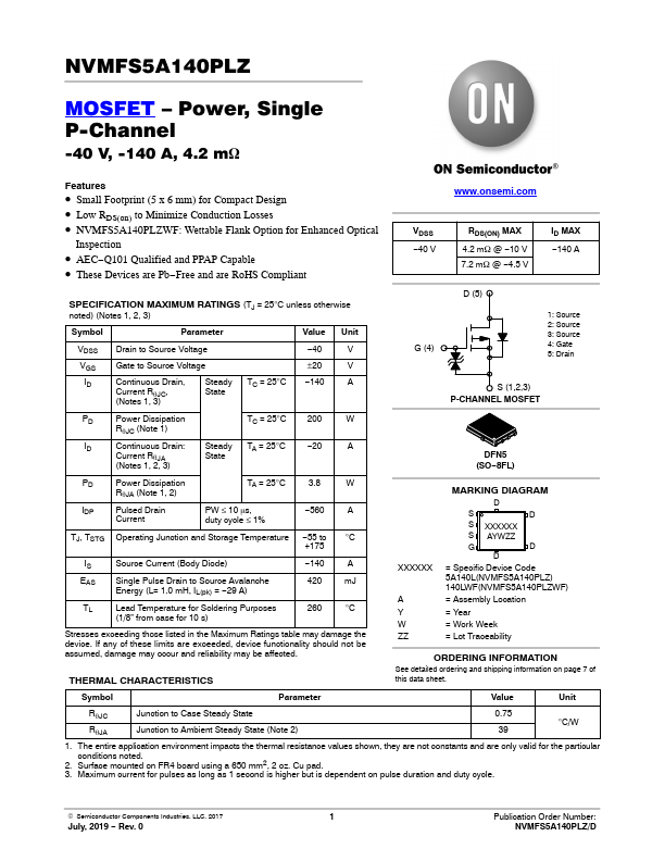
D (5) G (4)
1: Source 2: Source 3: Source 4: Gate 5: Drain
S (1,2,3) P-CHANNEL
MOSFET
PD Power Dissipation RqJC (Note 1)
TC = 25°C
200
ID
Continuous Drain: Steady TA = 25°C
−20
C(Nuorrteesnt1R, 2qJ,A3)
State
W A
DFN5 (SO−8FL)
PD Power Dissipation RqJA (Note 1, 2)
TA = 25°C
3.8
W
IDP Pulsed Drain Current
PW ≤ 10 ms, duty cycle ≤ 1%
−560
A
TJ, TSTG Operating Junction and Storage Temperature
−55 to +175
°C
IS Source Current (Body Diode) EAS Single Pulse Drain to Source Avalanche
Energy (L= 1.0 mH, IL(pk) = −29 A) TL Lead Temperature for Soldering Purposes
(1/8” from case for 10 s)
−140 420
A mJ
260 °C
Stresses exceeding those listed in the Maximum Ratings table may damage the device. If any of these limits are exceeded, device functionality should not be assumed, damage may occu...