DATA SHEET www.onsemi.com
MOSFET - Power, Single N-Channel
80 V, 3.2 mW, 135 A
V(BR)DSS 80 V
RDS(ON) MAX 3.2 mW @ 10 ...
DATA SHEET www.onsemi.com
MOSFET - Power, Single N-Channel
80 V, 3.2 mW, 135 A
V(BR)DSS 80 V
RDS(ON) MAX 3.2 mW @ 10 V 4.1 mW @ 4.5 V
ID MAX 135 A
NVMFS6H818NL
Features
Small Footprint (5x6 mm) for Compact Design Low RDS(on) to Minimize Conduction Losses Low QG and Capacitance to Minimize Driver Losses NVMFS6H818NLWF − Wettable Flank Option for Enhanced Optical
Inspection
AEC−Q101 Qualified and PPAP Capable These Devices are Pb−Free and are RoHS Compliant
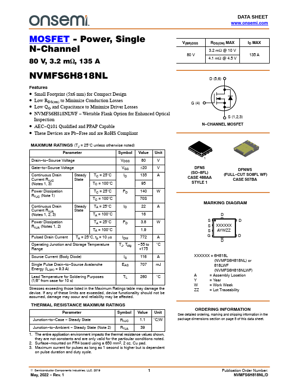
D (5,6)
G (4) S (1,2,3)
N−CHANNEL
MOSFET
MAXIMUM RATINGS (TJ = 25°C unless otherwise noted)
Parameter
Symbol Value Unit
Drain−to−Source
Voltage
VDSS
80
V
Gate−to−Source
Voltage
VGS
±20
V
Continuous Drain Current RqJC (Notes 1, 3)
Steady TC = 25°C
ID
State
TC = 100°C
135
A
95
Power Dissipation RqJC (Note 1)
TC = 25°C
PD
TC = 100°C
140 W 70S
Continuous Drain Current RqJA (Notes 1, 2, 3)
Steady TA = 25°C
ID
State
TA = 100°C
22
A
16
Power Dissipation RqJA (Notes 1, 2)
TA = 25°C
PD
TA = 100°C
3.8
W
1.9
Pulsed Drain Current TA = 25°C, tp = 10 ms
IDM
772
A
Operating Junction and Storage Temperature Range
TJ, Tstg − 55 to °C +175
Source Current (Body Diode)
Single Pulse Drain−to−Source Avalanche Energy (IL(pk) = 9.3 A)
Lead Temperature for Soldering Purposes (1/8″ from case for 10 s)
IS
116
A
EAS
707 mJ
TL
260 °C
Stresses exceeding those listed in the Maximum Ratings table may damage the device. If any of these limits are exceeded, device functionality should no...