OCO-SMBS
SMD OCXO Sine wave
Features
Applications: GPS, CDMA, 3G, networking, instrumentation SMD packaged preci...
OCO-SMBS
SMD OCXO Sine wave
Features
Applications: GPS, CDMA, 3G, networking, instrumentation SMD packaged precision OCXO High frequency stability vs. temperature Supply
voltage: 3.3 V or 5.0 V
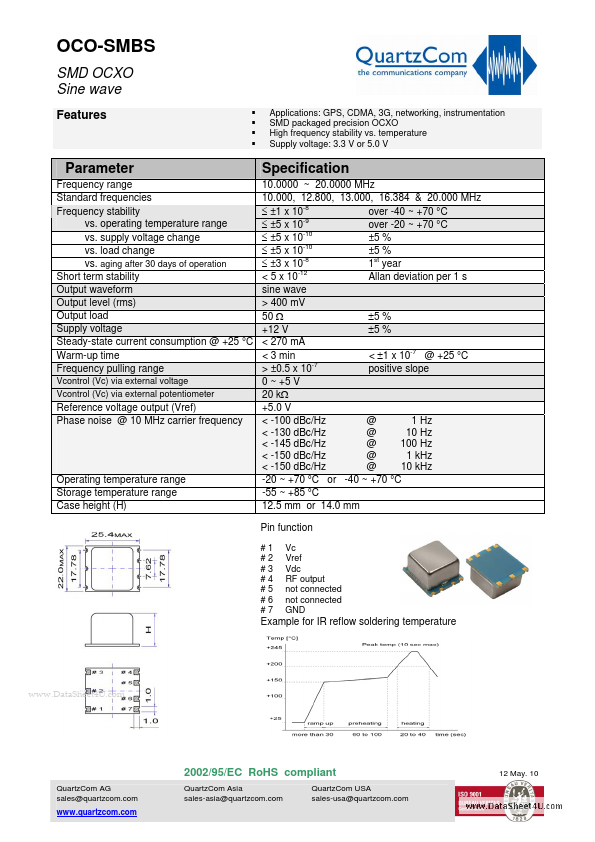
Parameter
Frequency range Standard frequencies Frequency stability vs. operating temperature range vs. supply
voltage change vs. load change vs. aging after 30 days of operation Short term stability Output waveform Output level (rms) Output load Supply
voltage Steady-state current consumption @ +25 °C Warm-up time Frequency pulling range
Vcontrol (Vc) via external
voltage Vcontrol (Vc) via external potentiometer
Specification
10.0000 ~ 20.0000 MHz 10.000, 12.800, 13.000, 16.384 & 20.000 MHz ±1 x 10⁻⁸ over -40 ~ +70 °C -9 ±5 x 10 over -20 ~ +70 °C ±5 % ±5 x 10⁻¹⁰ ±5 % ±5 x 10⁻¹⁰ 1st year ±3 x 10⁻⁸ -12 < 5 x 10 Allan deviation per 1 s sine wave > 400 mV 50 5 % +12 V 5 % < 270 mA < 3 min < 1 x 10⁻⁷ @ +25 °C -7 > ±0.5 x 10 positive slope 0 ~ +5 V 20 k +5.0 V < -100 dBc/Hz @ 1 Hz < -130 dBc/Hz @ 10 Hz < -145 dBc/Hz @ 100 Hz < -150 dBc/Hz @ 1 kHz < -150 dBc/Hz @ 10 kHz -20 ~ +70 °C or -40 ~ +70 °C -55 ~ +85 °C 12.5 mm or 14.0 mm Pin function
#1 #2 #3 #4 #5 #6 #7 Vc Vref Vdc RF output not connected not connected GND
Reference
voltage output (Vref) Phase noise @ 10 MHz carrier frequency
Operating temperature range Storage temperature range Case height (H)
Example for IR reflow soldering temperature
www.DataSheet4U.com
2002/95/EC RoHS compliant
QuartzCom AG sales@...