NIKO-SEM
N- & P-Channel Enhancement Mode Field Effect Transistor
P2503NPG
DIP-8
Halogen-Free & Lead-Free
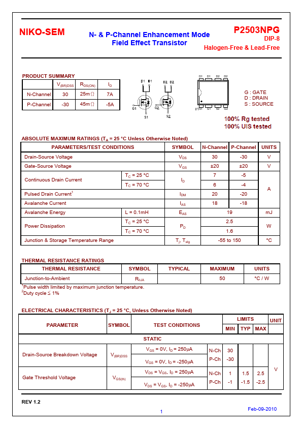
PRODUCT SUM...
NIKO-SEM
N- & P-Channel Enhancement Mode Field Effect Transistor
P2503NPG
DIP-8
Halogen-Free & Lead-Free
PRODUCT SUMMARY V(BR)DSS RDS(ON)
N-Channel 30 25mΩ P-Channel -30 45mΩ
ID 7A -5A
D1 D1 D2 D2
#1S1 G1 S2 G2
G : GATE D : DRAIN S : SOURCE
ABSOLUTE MAXIMUM RATINGS (TA = 25 °C Unless Otherwise Noted)
PARAMETERS/TEST CONDITIONS
SYMBOL
Drain-Source
Voltage Gate-Source
Voltage
Continuous Drain Current Pulsed Drain Current1 Avalanche Current Avalanche Energy
Power Dissipation
Junction & Storage Temperature Range
TC = 25 °C TC = 70 °C
L = 0.1mH TC = 25 °C TC = 70 °C
VDS VGS
ID
IDM IAS EAS
PD
Tj, Tstg
N-Channel P-Channel UNITS
30 -30 V
±20 ±20 V
7 -5
6 -4 A
20 -20
18 -18
19 mJ
2.5 W
1.6
-55 to 150
°C
THERMAL RESISTANCE RATINGS THERMAL RESISTANCE
SYMBOL
Junction-to-Ambient
RθJA
1Pulse width limited by maximum junction temperature.
2Duty cycle ≤ 1%
TYPICAL
MAXIMUM 50
UNITS °C / W
ELECTRICAL CHARACTERISTICS (TJ = 25 °C, Unless Otherwise Noted)
PA...