P261ALV
Dual P-Channel Enhancement Mode MOSFET
PRODUCT SUMMARY
V(BR)DSS
RDS(ON)
-12V
19mΩ @VGS = -4.5V
ID -8.5A
S...
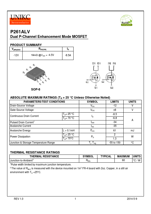
P261ALV
Dual P-Channel Enhancement Mode
MOSFET
PRODUCT SUMMARY
V(BR)DSS
RDS(ON)
-12V
19mΩ @VGS = -4.5V
ID -8.5A
SOP-8
ABSOLUTE MAXIMUM RATINGS (TA = 25 °C Unless Otherwise Noted)
PARAMETERS/TEST CONDITIONS
SYMBOL
LIMITS
Drain-Source
Voltage
VDS -12
Gate-Source
Voltage
VGS ±8
Continuous Drain Current Pulsed Drain Current1
TA= 25 °C TA= 70 °C
ID IDM
-8.5 -6.8 -34
Avalanche Current
IAS -35
Avalanche Energy
L = 0.1mH
EAS
61
Power Dissipation
TA= 25 °C TA= 70°C
PD
2 1.3
Junction & Storage Temperature Range
Tj, Tstg
-55 to 150
UNITS V V
A
mJ W °C
THERMAL RESISTANCE RATINGS
THERMAL RESISTANCE
SYMBOL
TYPICAL MAXIMUM
Junction-to-Ambient2
RqJA
60
1Pulse width limited by maximum junction temperature.
2 The value of RθJA is measured with the device mounted on 1in2 FR-4 board with 2oz. Copper, in a still air
environment with TA =25°C.
UNITS °C / W
REV 1.0
1 2014-5-9
P261ALV
Dual P-Channel Enhancement Mode
MOSFET
ELECTRICAL CHARACTERISTICS (...