(P8M648YLx / P8M6416YLEx) 8M/16M x 64 DIMM SDRAM Module
P8M648YL, P16M6416YL
Preliminary Release V1
SDRAM MODULE
Features:
• • • • • • • • •
P8M648YLE, P16M6416YLE 8M, 16M x ...
Description
P8M648YL, P16M6416YL
Preliminary Release V1
SDRAM MODULE
Features:
P8M648YLE, P16M6416YLE 8M, 16M x 64 DIMM
PC-100 and PC133 Compatible JEDEC – Standard 168-pin , dual in-line memory Module (DIMM) TSOP components. Single 3.3v +.3v power supply. Nonbuffered fully synchronous; all signals measured on positive edge of system clock. Internal pipelined operation; column address can be changed every clock cycle. Quad internal banks for hiding row access/precharge. 64ms 4096 cycle refresh. All inputs, outputs, clocks LVTTL compatible.
PIN
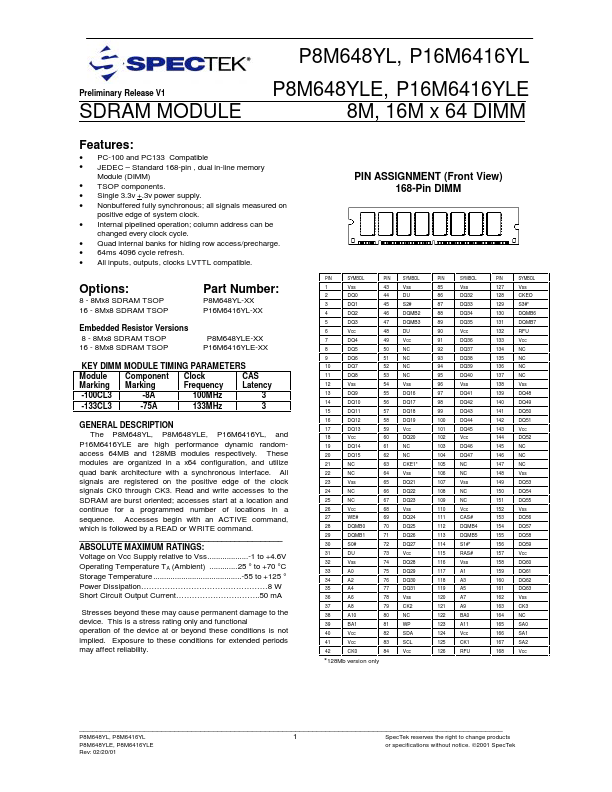
PIN ASSIGNMENT (Front View) 168-Pin DIMM
SYMBOL
PIN
SYMBOL
PIN
SYMBOL
PIN
SYMBOL
Options:
8 - 8Mx8 SDRAM TSOP 16 - 8Mx8 SDRAM TSOP Embedded Resistor Versions 8 - 8Mx8 SDRAM TSOP 16 - 8Mx8 SDRAM TSOP
Part Number:
P8M648YL-XX P16M6416YL-XX
P8M648YLE-XX P16M6416YLE-XX
KEY DIMM MODULE TIMING PARAMETERS Module Component Clock CAS Marking Marking Frequency Latency -100CL3 -8A 100MHz 3 -133CL3 -75A 133MHz 3 GENERAL DESCRIPTION The P8M648YL, P8M648YLE, P16M6416YL, and P16M6416YLE are high performance dynamic randomaccess 64MB and 128MB modules respectively. These modules are organized in a x64 configuration, and utilize quad bank architecture with a synchronous interface. All signals are registered on the positive edge of the clock signals CK0 through CK3. Read and write accesses to the SDRAM are burst oriented; accesses start at a location and continue for a programmed number of locations in a sequence. Accesses begin with...
Similar Datasheet