PPJA3412
20V N-Channel Enhancement Mode
MOSFET
Voltage
20 V
Current
4.1A
Features
RDS(ON) ,
[email protected],
[email protected]<56mΩ RDS(ON) ,
[email protected],
[email protected]<68mΩ RDS(ON) ,
[email protected],
[email protected]<95mΩ Advanced Trench Process Technology Specially Designed for Switch Load, PWM Application, etc. Lead free in compliance with EU RoHS 2011/65/EU
directive. Green molding compound as per IEC61249 Std.
(Halogen Free)
Mechanical Data
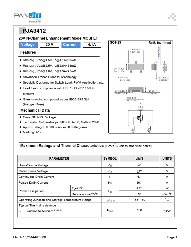
Case: SOT-23 Package Terminals : Solderable per MIL-STD-750, Method 2026 Approx. Weight: 0.0003 ounces, 0.0084 grams Marking: A12
SOT-23
Unit: inch(mm)
Maximum Ratings and Thermal Characteristics (TA=25oC unless otherwise noted)
PARAMETER
Drain-Source
Voltage
Gate-Source
Voltage
Continuous Drain Current
Pulsed Drain Current Power Dissipation
Ta=25oC Derate above 25oC
Operating Junction and Storage Temperature Range
Typical Thermal resistance - Junction to Ambient (Note 3)
SYMBOL VDS VGS ID IDM
PD
TJ,TSTG
RθJA
LIMIT 20 +12 4.1 16.4 1.25 10
-55~150
100
UNITS V V A A W
mW/ oC oC
oC/W
March 10,2014-REV.00
Page 1
PPJA3412
Electrical Characteristics (TA=25oC unless otherwise noted)
PARAMETER Static Drain-Source Breakdown
Voltage Gate Threshold
Voltage
Drain-Source On-State Resistance
Zero Gate
Voltage Drain Current Gate-Source Leakage Current Dynamic Total Gate Charge Gate-Source Charge Gate-Drain Charge Input Capacitance Output Capacitance Reverse Transfer Capacitance Switching Turn-On Delay Time Turn-On Rise Time Turn-Off Delay Time ...