PL502-35/-37/-38/-39
750kHz – 800MHz Low Phase Noise Multiplier VCXO
Universal Low Phase Noise ICs
FEATURES
PIN CONFI...
PL502-35/-37/-38/-39
750kHz – 800MHz Low Phase Noise Multiplier VCXO
Universal Low Phase Noise ICs
FEATURES
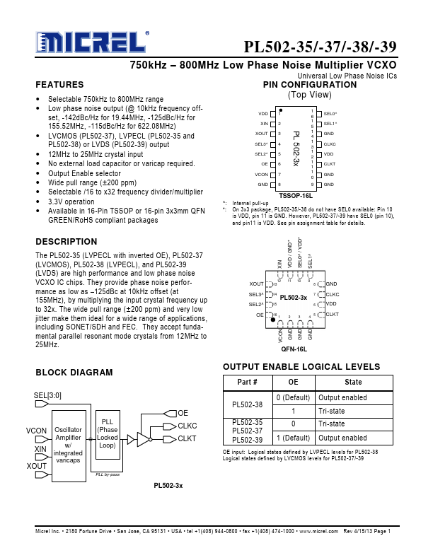
PIN CONFIGURATION
Selectable 750kHz to 800MHz range Low phase noise output (@ 10kHz frequency off-
set, -142dBc/Hz for 19.44MHz, -125dBc/Hz for 155.52MHz, -115dBc/Hz for 622.08MHz) LV
CMOS (PL502-37), LVPECL (PL502-35 and PL502-38) or LVDS (PL502-39) output 12MHz to 25MHz crystal input No external load capacitor or varicap required. Output Enable selector Wide pull range (±200 ppm) Selectable /16 to x32 frequency divider/multiplier 3.3V operation Available in 16-Pin TSSOP or 16-pin 3x3mm QFN GREEN/RoHS compliant packages
(Top View)
VDD XIN XOUT SEL3^ SEL2^ OE VCON GND
1 2 3 4 5 6 7 8
PL 502-3x
1 6
SEL0^
1 5
SEL1^
1 4
GND
1 3
CLKC
1 2
VDD
1 1
CLKT
1 0
GND
9 GND
TSSOP-16L
^: Internal pull-up *: On 3x3 package, PL502-35/-38 do not have SEL0 available: Pin 10
is VDD, pin 11 is GND. However, PL502-37/-39 have SEL0 (pin 10), and pin11 is VDD. See pin assignment table for details.
XIN VDD / GND* SEL0^ / VDD* SEL1^
DESCRIPTION
The PL502-35 (LVPECL with inverted OE), PL502-37 (LV
CMOS), PL502-38 (LVPECL), and PL502-39 (LVDS) are high performance and low phase noise VCXO IC chips. They provide phase noise performance as low as –125dBc at 10kHz offset (at 155MHz), by multiplying the input crystal frequency up to 32x. The wide pull range (±200 ppm) and very low jitter make them ideal for a wide range of applications, including SONET/SDH a...