PL520-80
Low Phase Noise VCXO (9.5-65MHz)
FEATURES
19MHz to 65MHz fundamental crystal input. Output range: 9.5MHz ...
PL520-80
Low Phase Noise VCXO (9.5-65MHz)
FEATURES
19MHz to 65MHz fundamental crystal input. Output range: 9.5MHz – 65MHz Complementary outputs: PECL or LVDS output. Selectable OE Logic (enable high or enable low). Available outputs: PECL, LVDS, or
CMOS (High
Drive (30mA) or Standard Drive (10mA) output). Integrated variable
capacitors. Supports 2.5V or 3.3V Power Supply. Available in die form.
DESCRIPTION The PL520-80 is a VCXO IC specifically designed to work with fundamental crystals between 19MHz and 65MHz. The selectable divide by two feature extends the operation range from 9.5MHz to 65MHz. It requires very low current into the crystal resulting in better overall stability. The OE logic feature allows selection of enable high or enable low. Furthermore, it provides selectable
CMOS, PECL or LVDS outputs.
DIE SPECIFICATIONS
Name
Size Reverse side Pad dimensions
Th ic kn e s s
Value
62 x 65 mil GND
80 m icron x 80 micron 10 mil
BLOCK DIAGRAM
VCON Oscillator
Amplifier w/
XIN integrated
varicaps
XOUT
OE Q Q
S2 PL520-80
62 mil
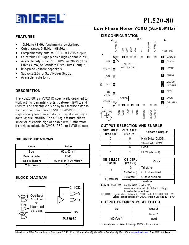
DIE CONFIGURATION
65 mil
OUTSEL0^ VDD VDD VDD VDD N/C Reserved OUTSEL1^
25 24 23 22 21 20 19 18
XIN 26 XOUT 27
Die ID: A2020-20C
N/C 28
S2^ 29
OE 30
CTRL
VCON 31
C502A
12345 6 78
(1550,1475) 17 GNDBUF 16
CMOS
15 LVDSB
14 PECLB
13 VDDBUF 12 VDDBUF 11 PECL
10 LVDS 9 OE_SEL^
Y (0,0) X
GND GND GND GND GND Reserved GNDBUF GNDBUF
OUTPUT SELECTION AND ENABLE
OUT_SEL1* OUT_SEL0*
(Pad 18)
(Pad 25)
Selected Output*
0 0...