2.5V/3.3V QUAD 2:1 MUX/DEMUX HIGH BANDWIDTH BUS SWITCH
IDTQS3VH257 2.5V / 3.3V QUAD 2:1 MUX/DEMUX HIGH BANDWIDTH BUS SWITCH
INDUSTRIAL TEMPERATURE RANGE
QUICKSWITCH® PRODUCT...
Description
IDTQS3VH257 2.5V / 3.3V QUAD 2:1 MUX/DEMUX HIGH BANDWIDTH BUS SWITCH
INDUSTRIAL TEMPERATURE RANGE
QUICKSWITCH® PRODUCTS 2.5V/3.3V QUAD 2:1 MUX/DEMUX HIGH BANDWIDTH BUS SWITCH
IDTQS3VH257
FEATURES:
N channel FET switches with no parasitic diode to VCC – Isolation under power-off conditions – No DC path to VCC or GND – 5V tolerant in OFF and ON state
5V tolerant I/Os Low RON - 4Ω typical Flat RON characteristics over operating range Rail-to-rail switching 0 - 5V Bidirectional dataflow with near-zero delay: no added ground
bounce Excellent RON matching between channels VCC operation: 2.3V to 3.6V High bandwidth - up to 500MHz LVTTL-compatible control Inputs Undershoot Clamp Diodes on all switch and control Inputs Low I/O capacitance, 4pF typical Available in QSOP, SOIC, and TSSOP packages
APPLICATIONS:
Hot-swapping Multiplexing/demultiplexing Low distortion analog switch Replaces mechanical relay ATM 25/155 switching
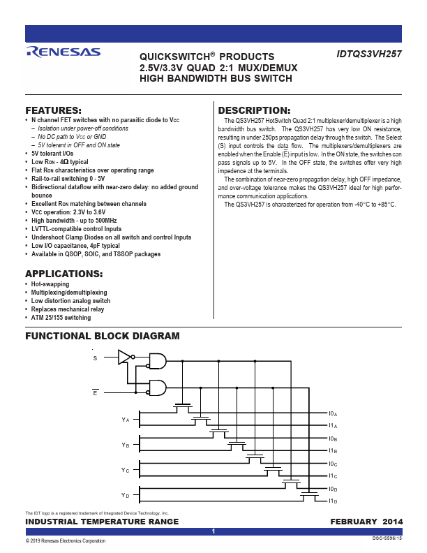
FUNCTIONAL BLOCK DIAGRAM
S
DESCRIPTION:
The QS3VH257 HotSwitch Quad 2:1 multiplexer/demultiplexer is a high bandwidth bus switch. The QS3VH257 has very low ON resistance, resulting in under 250ps propagation delay through the switch. The Select (S) input controls the data flow. The multiplexers/demultiplexers are enabled when the Enable (E) input is low. In the ON state, the switches can pass signals up to 5V. In the OFF state, the switches offer very high impedence at the terminals.
The combination of near-zero propagation d...
Similar Datasheet