Preliminary Datasheet
RJK03P7DPA
MOS1 30 V, 15 A, 9.4 mΩ max. MOS2 30 V, 30 A, 5.3 mΩ max. Built in SBD Dual N-channel ...
Preliminary Datasheet
RJK03P7DPA
MOS1 30 V, 15 A, 9.4 mΩ max. MOS2 30 V, 30 A, 5.3 mΩ max. Built in SBD Dual N-channel Power MOS FET High Speed Power Switching
R07DS0906EJ0110 Rev.1.10
Nov 01, 2012
Features
Low on-resistance Capable of 4.5 V gate drive High density mounting Pb-free Halogen-free
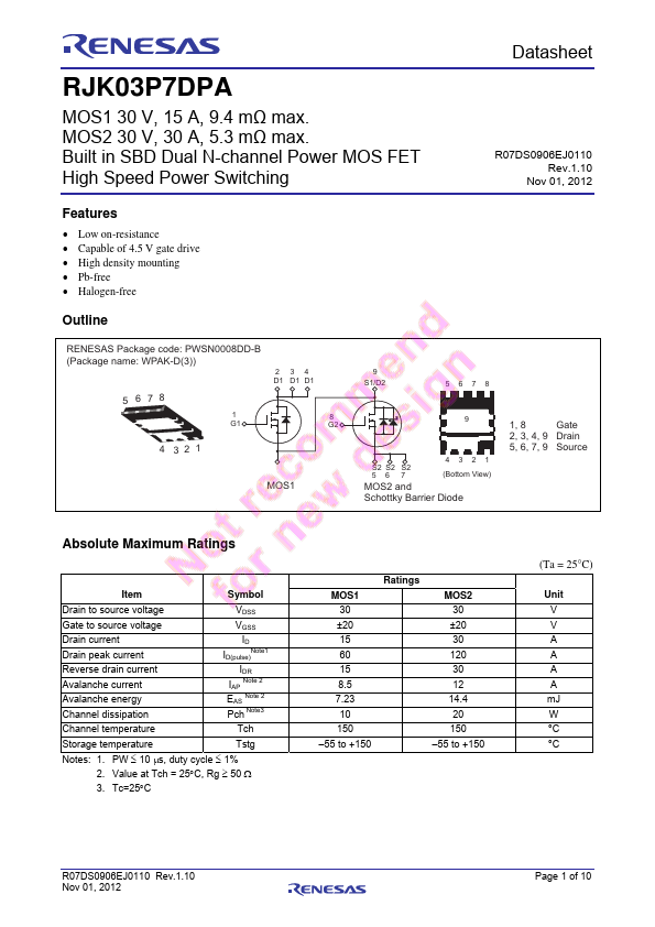
Outline
RENESAS Package code: PWSN0008DD-B (Package name: WPAK-D(3))
5 678
1 G1
234 D1 D1 D1
8 G2
4 32 1
MOS1
9 S1/D2
5678
9
S2 S2 S2 56 7
4321 (Bottom View)
MOS2 and
Schottky Barrier Diode
1, 8 Gate 2, 3, 4, 9 Drain 5, 6, 7, 9 Source
Absolute Maximum Ratings
Item
Symbol
Drain to source
voltage Gate to source
voltage Drain current Drain peak current Reverse drain current Avalanche current Avalanche energy Channel dissipation
VDSS
VGSS
ID ID(pulse)Note1
IDR IAP Note 2 EAS Note 2 Pch Note3
Channel temperature
Tch
Storage temperature
Tstg
Notes: 1. PW 10 s, duty cycle 1% 2. Value at Tch = 25C, Rg 50
3. Tc=25C
MOS1 30 ±20 15 60 15 8.5 7.23 10 150
–55 to +150
Ratings
MOS2 30 ±20 30 120 30 12 14.4 20 150
–55 to +150
(Ta = 25°C)
Unit V V A A A A mJ W
°C °C
R07DS0906EJ0110 Rev.1.10 Nov 01, 2012
Page 1 of 10
RJK03P7DPA
Electrical Characteristics
MOS1
Item Drain to source breakdown
voltage Gate to source leak current Zero gate
voltage drain current Gate to source cutoff
voltage Static drain to source on state resistance
Forward transfer admittance Input capacitance Output capacitance Reverse transfer capacitance Gate Resistance Total ...