RJK0630JPE
Silicon N Channel MOS FET High Speed Power Switching
Features
• For Automotive application • AEC-Q101 complia...
RJK0630JPE
Silicon N Channel MOS FET High Speed Power Switching
Features
For Automotive application AEC-Q101 compliant Low on-resistance : RDS(on) = 6.2 mΩ typ. Capable of 4.5 V gate drive Low input capacitance : Ciss = 2100 pF typ.
Outline
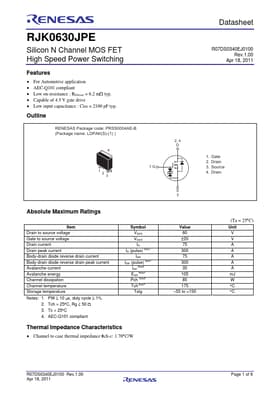
RENESAS Package code: PRSS0004AE-B (Package name: LDPAK(S)-(1) )
4
123
1G
Absolute Maximum Ratings
Item Drain to source
voltage Gate to source
voltage Drain current Drain peak current Body-drain diode reverse drain current Body-drain diode reverse drain peak current Avalanche current Avalanche energy Channel dissipation Channel temperature Storage temperature Notes: 1. PW ≤ 10 μs, duty cycle ≤ 1%
2. Tch = 25°C, Rg ≥ 50 Ω 3. Tc = 25°C 4. AEC-Q101 compliant
Symbol
VDSS
VGSS
ID ID (pulse) Note1
IDR IDR (pulse) Note1
I Note2
AP
E Note2
AR
Pch Note3 Tch Note4
Tstg
Thermal Impedance Characteristics
Channel to case thermal impedance θch-c: 1.76°C/W
Preliminary Datasheet
R07DS0340EJ0100 Rev.1.00
Apr 18, 2011
2, 4 D
1. Gate 2. Drain 3. Source 4. Drain
S 3
Value 60 ±20 75 300 75 300 35 105 85 175
–55 to +150
(Ta = 25°C)
Unit V V A A A A A mJ W °C °C
R07DS0340EJ0100 Rev.1.00 Apr 18, 2011
Page 1 of 6
RJK0630JPE
Electrical Characteristics
Item Gate to source leak current Zero gate
voltage drain current Gate to source cutoff
voltage Static drain to source on state resistance Input capacitance Output capacitance Reverse transfer capacitance Total gate charge Gate to source charge Gate to drain charge Turn-on delay time Rise time...