RQJ0301HGDQS
Silicon P Channel MOS FET Power Switching
Features
• Low on-resistance RDS(on) = 38 m Ω typ (VGS = –10 V, I...
RQJ0301HGDQS
Silicon P Channel MOS FET Power Switching
Features
Low on-resistance RDS(on) = 38 m Ω typ (VGS = –10 V, ID = –2.6 A)
Low drive current High speed switching 4.5 V gate drive
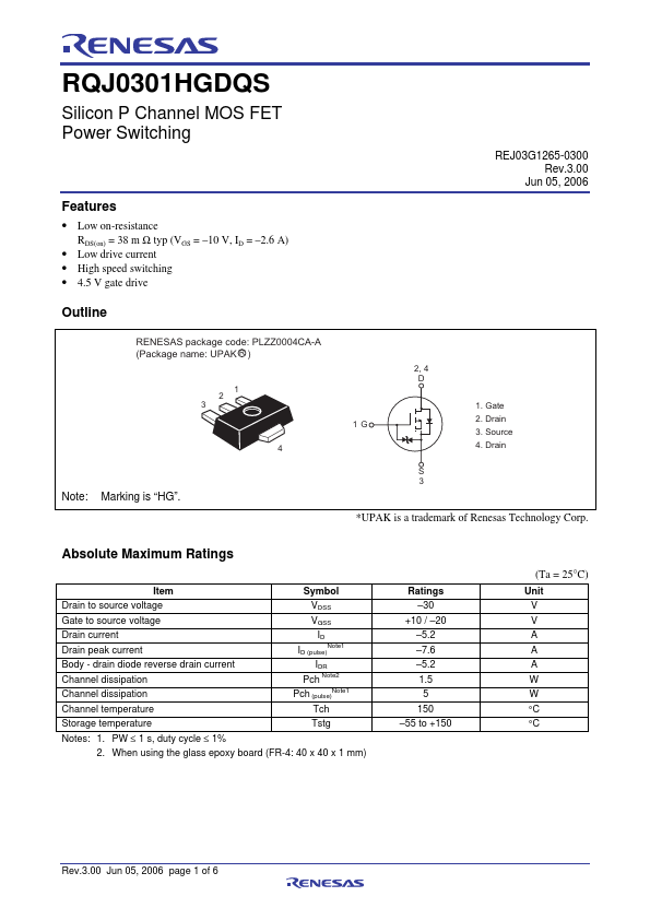
Outline
RENESAS package code: PLZZ0004CA-A (Package name: UPAK R )
1 2 3
4
Note: Marking is “HG”.
REJ03G1265-0300 Rev.3.00
Jun 05, 2006
2, 4 D
1. Gate 1 G 2. Drain
3. Source 4. Drain S 3
*UPAK is a trademark of Renesas Technology Corp.
Absolute Maximum Ratings
Item
Symbol
Drain to source
voltage
VDSS
Gate to source
voltage
VGSS
Drain current Drain peak current
ID
ID
Note1 (pulse)
Body - drain diode reverse drain current Channel dissipation Channel dissipation
IDR
Pch Note2
Pch
Note1 (pulse)
Channel temperature
Tch
Storage temperature
Tstg
Notes: 1. PW ≤ 1 s, duty cycle ≤ 1%
2. When using the glass epoxy board (FR-4: 40 x 40 x 1 mm)
Ratings –30
+10 / –20 –5.2 –7.6 –5.2 1.5 5 150
–55 to +150
(Ta = 25°C)
Unit V V A A A W W °C °C
Rev.3.00 Jun 05, 2006 page 1 of 6
RQJ0301HGDQS
Electrical Characteristics
Item Drain to source breakdown
voltage Gate to source breakdown
voltage Gate to source breakdown
voltage Gate to source leak current Gate to source leak current Drain to source leak current Gate to source cutoff
voltage Drain to source on state resistance
Forward transfer admittance Input capacitance Output capacitance Reverse transfer capacitance Turn - on delay time Rise time Turn - off delay time Fall time Total gate charge Gate to source charge Gate to drain ...