![]() |
MOSFET. RUF025N02 Datasheet |
|
![]() RUF025N02
Nch 20V 2.5A Power MOSFET
Datasheet
VDSS
RDS(on) (Max.)
ID
PD
20V
54mW
2.5A
0.8W
lFeatures
1) Low on - resistance.
2) 1.5V Drive.
3) Built-in G-S Protection Diode.
4) Small Surface Mount Package (TUMT3).
5) Pb-free lead plating ; RoHS compliant
lApplication
DC/DC converters
lAbsolute maximum ratings(Ta = 25°C)
Parameter
Drain - Source voltage
Continuous drain current
Pulsed drain current
Gate - Source voltage
Power dissipation
Junction temperature
Range of storage temperature
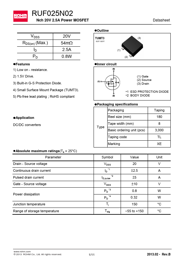
lOutline
TUMT3
SOT-323T
(1)
(2)
lInner circuit
(3)
(1) Gate
(2) Source
(3) Drain
*1 ESD PROTECTION DIODE
*2 BODY DIODE
lPackaging specifications
Packaging
Reel size (mm)
Tape width (mm)
Type
Basic ordering unit (pcs)
Taping code
Marking
Taping
180
8
3,000
TL
XE
Symbol
VDSS
ID *1
ID,pulse *2
VGSS
PD *3
PD *4
Tj
Tstg
Value
20
2.5
5
10
0.8
0.32
150
-55 to +150
Unit
V
A
A
V
W
W
°C
°C
www.rohm.com
© 2013 ROHM Co., Ltd. All rights reserved.
1/11
2013.02 - Rev.B
|
|
![]() RUF025N02
lThermal resistance
Parameter
Thermal resistance, junction - ambient
Data Sheet
Symbol
RthJA *3
RthJA *4
Values
Min. Typ. Max.
Unit
- - 156 °C/W
- - 391 °C/W
lElectrical characteristics(Ta = 25°C)
Parameter
Symbol
Conditions
Drain - Source breakdown
voltage
V(BR)DSS VGS = 0V, ID = 1mA
Values
Min. Typ. Max.
Unit
20 - - V
Breakdown voltage
temperature coefficient
ΔV(BR)DSS ID=1mA
ΔTj referenced to 25°C
Zero gate voltage drain current
Gate - Source leakage current
Gate threshold voltage
IDSS
IGSS
VGS (th)
VDS = 20V, VGS = 0V
VGS = 10V, VDS = 0V
VDS = 10V, ID = 1mA
Gate threshold voltage
temperature coefficient
ΔV(GS)th ID=1mA
ΔTj referenced to 25°C
Static drain - source
on - state resistance
Gate input resistannce
Transconductance
VGS=4.5V, ID=2.5A
VGS=2.5V, ID=2.5A
RDS(on) *5 VGS=1.8V, ID=1.3A
VGS=1.5V, ID=0.5A
VGS=4.5V, ID=2.5A, Tj=125°C
RG
gfs *5
f = 1MHz, open drain
VDS=10V, ID=2.5A
*1 Limited only by maximum temperature allowed.
*2 Pw 10ms, Duty cycle 1%
*3 Mounted on a seramic board (30×30×0.8mm)
*4 Mounted on a FR4 (15×20×0.8mm)
*5 Pulsed
-
-
-
0.3
-
-
-
-
-
-
-
3.6
20
-
-
-
-1.9
39
49
65
80
65
7.5
6.0
- mV/°C
1 mA
10 mA
1.3 V
- mV/°C
54
68
91 mW
160
95
-W
-S
www.rohm.com
© 2013 ROHM Co., Ltd. All rights reserved.
2/11
2013.02 - Rev.B
|
![]() RUF025N02
Data Sheet
lElectrical characteristics(Ta = 25°C)
Parameter
Symbol
Conditions
Input capacitance
Output capacitance
Reverse transfer capacitance
Turn - on delay time
Rise time
Turn - off delay time
Fall time
Ciss
Coss
Crss
td(on) *5
tr *5
td(off) *5
tf *5
VGS = 0V
VDS = 10V
f = 1MHz
VDD ⋍ 10V, VGS = 4.5V
ID = 1.3A
RL = 7.7W
RG = 10W
Values
Min. Typ. Max.
- 370 -
- 90 -
- 50 -
-7-
- 15 -
- 35 -
- 15 -
Unit
pF
ns
lGate Charge characteristics(Ta = 25°C)
Parameter
Symbol
Conditions
Total gate charge
Gate - Source charge
Gate - Drain charge
Qg *5
Qgs *5
Qgd *5
VDD ⋍ 10V, ID=2.5A
VGS = 4.5V
Values
Min. Typ. Max.
-5-
- 0.9 -
- 0.8 -
Unit
nC
lBody diode electrical characteristics (Source-Drain)(Ta = 25°C)
Parameter
Symbol
Conditions
Min.
Values
Typ.
Max.
Inverse diode continuous,
forward current
Forward voltage
IS *1 Ta = 25°C
VSD *5 VGS = 0V, Is = 0.6A
- - 0.6
- - 1.2
Unit
A
V
www.rohm.com
© 2013 ROHM Co., Ltd. All rights reserved.
3/11
2013.02 - Rev.B
|
@ 2014 :: Datasheetspdf.com :: Semiconductors datasheet search & download site (Privacy Policy & Contact) |