INVERTER
S-75V04ANC
n General Description
The S-75V04ANC is a INVERTER fabricated by utilizing advanced silicon-gate C...
INVERTER
S-75V04ANC
n General Description
The S-75V04ANC is a INVERTER fabricated by utilizing advanced silicon-gate
CMOS technology which provides the inherent benefit of
CMOS low power consumption to achieve ultra high speed operation correspond to LSTTL IC’s. All gates of the internal circuitry have buffered outputs to ensure high noise immunity and output stability. Input
voltage is allowed to be applied even if power
voltage is not supplied because no diode is inserted between an input pin and VCC. This allows for interfaces between power supplies of different
voltage, output level conversion from 5 V to 3 V and battery backup applications.
n Features
Ÿ Wide power supply range: 2 V to 5.5 V
Ÿ Low current consumption: 1.0 µA max. (at 5.5 V, 25°C)
Ÿ Typical propagation delay: tpd = 3.8 ns (at 5 V)
Ÿ High noise immunity: Ÿ Power down protection:
VNIH=VNIL=28% VCC minimum All pins
Ÿ Very small plastic package: SC-88A
n Applications
Ÿ Personal computers, peripherals
Ÿ Cellular phones Ÿ Cameras Ÿ Games
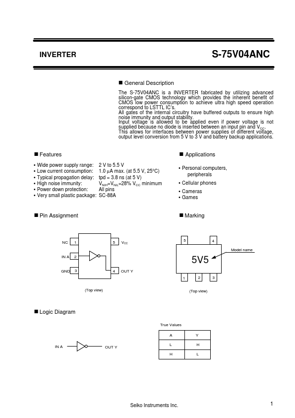
n Pin Assignment
n Marking
NC 1 IN A 2 GND 3
5 VCC 4 OUT Y
(Top view)
n Logic Diagram
IN A
OUT Y
54
5V5
1 23 (Top view)
Model name
True Values A L H
Y H L
Seiko Instruments Inc.
1
Miniaturized Logic IC Family S-75V04ANC n Physical Dimensions (Unit:mm)
SC-88A
2.0 ( 2.2 max.) 1.3±0.1
54
1.25 2.1±0.1
0.15
+0.1 −0.05
0.15 0.0 to 0.1
1 0.2 +0.1
−0.05
2
3 0.65
0.9±0.1
n Ordering
Delivery form: Taping only Model name: S-75V04ANC-5V5-T2
n Absolute Maxim...