INTEGRATED CIRCUITS
IN2 4
GND2 3
OUT2 2
VCC 1
AMP2
AMP1
5 ENABLE
6 IN1
7 GND1
8 OUT1
SA5200 RF dual gain-stag...
INTEGRATED CIRCUITS
IN2 4
GND2 3
OUT2 2
VCC 1
AMP2
AMP1
5 ENABLE
6 IN1
7 GND1
8 OUT1
SA5200 RF dual gain-stage
Product Specification Replaces data of Oct 10 1991 IC17 Data Handbook 1997 Nov 07
Philips Semiconductors
Philips Semiconductors
Product specification
RF dual gain-stage
SA5200
DESCRIPTION
The SA5200 is a dual amplifier with DC to 1200MHz response. Low noise (NF = 3.6dB) makes this part ideal for RF front-ends, and a simple power-down mode saves current for battery operated equipment. Inputs and outputs are matched to 50Ω. The enable pin allows the designer the ability to turn the
amplifiers on or off, allowing the part to act as an amplifier as well as an attenuator. This is very useful for front-end buffering in receiver applications.
PIN CONFIGURATION
D Package
1 2 3 4 8 7 6 5
VC
OUT1 GND1 IN1 ENABLE
C OUT2
GND2 IN2
FEATURES
Dual
amplifiers DC - 1200MHz operation Low DC power consumption (4.2mA per amplifier @ VCC = 5V) Power-Down Mode (ICC = 95µA typical) 3.6dB noise figure at 900MHz Unconditionally stable Fully ESD protected Low cost
ORDERING INFORMATION
DESCRIPTION 8-Pin Plastic Small Outline (Surface–mount)
SR00166
Supply
voltage 4-9V Gain S21 = 7dB at f = 1GHz Input and output match S11, S22 typically <–14dB
APPLICATIONS
Figure 1. Pin Configuration
Cellular radios RF IF strips Portable equipment
TEMPERATURE RANGE –40-+85°C ORDER CODE SA5200D DWG # SOT96-1
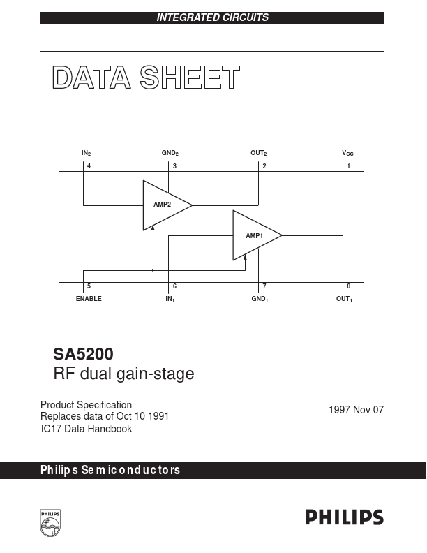
BLOCK DIAGRAM
IN2 4 GND2 3 OUT2 2 VCC 1
AMP2
AMP...