Elektronische Bauelemente
SDT517
N & P-Ch Enhancement Mode MOSFET N-Ch: 6A, 12V, RDS(ON) 24 mΩ
P-Ch: -4.1A, -12V, RDS(O...
Elektronische Bauelemente
SDT517
N & P-Ch Enhancement Mode
MOSFET N-Ch: 6A, 12V, RDS(ON) 24 mΩ
P-Ch: -4.1A, -12V, RDS(ON) 45 mΩ
RoHS Compliant Product A suffix of “-C” specifies halogen and lead-free
FEATURES
Surface Mount Package Super High Density Cell Design for Extremely Low RDS(ON) Exceptional On-resistance and Maximum DC Current Capability
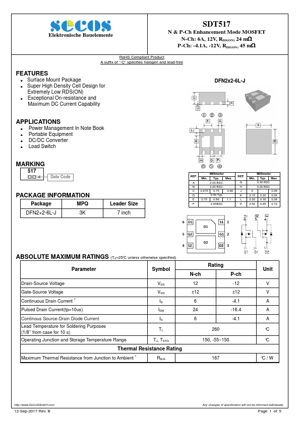
DFN2x2-6L-J
APPLICATIONS
Power Management In Note Book Portable Equipment DC/DC Converter Load Switch
MARKING
517
Date Code
PACKAGE INFORMATION
Package
MPQ
DFN2×2-6L-J
3K
Leader Size 7 inch
REF.
A B C D E F
Millimeter
Min. Typ. Max.
2.00 BSC.
2.00 BSC.
0.675 0.75
0.80
0.30 Typ.
0.75 0.86 1.1
0.65BSC
REF.
G H J K L P
Millimeter Min. Typ. Max.
0.30 BSC 0.20 BSC 0 -- 0.06 0.15 0.20 0.25 0.20 0.30 0.38
0.52 0.65 0.72
ABSOLUTE MAXIMUM RATINGS (TA=25°C unless otherwise specified)
Parameter
Symbol
Drain-Source
Voltage
VDS
Gate-Source
Voltage Continuous Drain Current 1
VGS ID
Pulsed Drain Current(tp=10us)
IDM
Continous Source-Drain Diode Current
Lead Temperature for Soldering Purposes (1/8’’ from case for 10 s)
IS TL
Operating Junction and Storage Temperature Range
TJ, TSTG
Thermal Resistance Rating
Maximum Thermal Resistance from Junction to Ambient 1
RθJA
N-ch 12 ±12 6 24 6
Rating
P-ch -12 ±12 -4.1 -16.4 -4.1
260
150, -55~150
167
Unit
V V A A A °C °C
°C / W
http://www.SeCoSGmbH.com/
12-Sep-2017 Rev. B
Any changes of specification will not be informed individually.
Page 1 of 5
Elektronische B...