P-Channel 1.8-V (G-S) MOSFET
Si2311DS
Vishay Siliconix
PRODUCT SUMMARY
VDS (V)
RDS(on) (Ω)
0.045 at VGS = - 4.5 V -...
P-Channel 1.8-V (G-S)
MOSFET
Si2311DS
Vishay Siliconix
PRODUCT SUMMARY
VDS (V)
RDS(on) (Ω)
0.045 at VGS = - 4.5 V - 8 0.072 at VGS = - 2.5 V
0.120 at VGS = - 1.8 V
ID (A) - 3.5 - 2.8 - 2.0
FEATURES Halogen-free Option Available TrenchFET® Power
MOSFET
APPLICATIONS Load Switch
RoHS
COMPLIANT
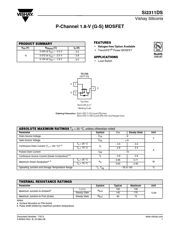
TO-236 (SOT-23)
G1 S2
3D
Top View Si2311DS (C1)* * Marking Code
Ordering Information: Si2311DS-T1-E3 (Lead (Pb)-free) Si2311DS-T1-GE3 (Lead (Pb)-free and Halogen-free)
ABSOLUTE MAXIMUM RATINGS TA = 25 °C, unless otherwise noted
Parameter
Symbol
5 s Steady State
Drain-Source
Voltage
VDS - 8
Gate-Source
Voltage
VGS
±8
Continuous Drain Current (TJ = 150 °C)a, b
TA = 25 °C TA = 70 °C
ID
- 3.5 - 2.8
- 3.0 - 2.4
Pulsed Drain Current
IDM - 10
Continuous Source Current (Diode Conduction)a, b
IS
- 0.8
- 0.6
Maximum Power Dissipationa, b
TA = 25 °C TA = 70 °C
PD
0.96 0.71 0.62 0.46
Operating Junction and Storage Temperature Range
TJ, Tstg
- 55 to 150
Unit V
A
W °C
THERMAL RESISTANCE RATINGS
Parameter Maximum Junction-to-Ambienta Maximum Junction-to-Foot (Drain)
t≤5s Steady State Steady State
Notes: a. Surface Mounted on FR4 board. b. Pulse width limited by maximum junction temperature.
Symbol RthJA RthJF
Document Number: 71813 S-80642-Rev. B, 24-Mar-08
Typical 100 140 60
Maximum 130 175 75
Unit °C/W
www.vishay.com 1
Si2311DS
Vishay Siliconix
SPECIFICATIONS TJ = 25 °C, unless otherwise noted
Parameter
Symbol
Test Conditions
Static
Drain-...