20V N-Channel Enhancement Mode
MOSFET
VDS= 20V RDS(ON),
[email protected],
[email protected] < 31mΩ RDS(ON),
[email protected],
[email protected] < 37mΩ RDS(ON),
[email protected],
[email protected] < 85mΩ
Features Advanced trench process technology High Density Cell Design For Ultra Low On-Resistance
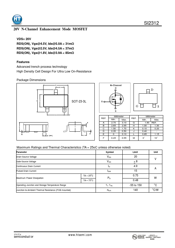
Package Dimensions
SI2312
D
SOT-23-3L
GS
REF.
A B C D E
F
Millimeter Min. Max. 2.70 3.10 2.65 2.95 1.50 1.70 0.35 0.50
0 0.10
0.45 0.55
REF.
G H K J L
M
Millimeter
Min. Max.
1.90 1.00 0.10 0.40 0.85
REF. 1.30 0.20 1.15
0° 10°
Maximum Ratings and Thermal Characteristics (TA = 25oC unless otherwise noted)
Parameter
Symbol
Limit
Drain-Source
Voltage Gate-Source
Voltage Continuous Drain Current Pulsed Drain Current
Maximum Power Dissipation
TA = 25oC TA = 75oC
VDS VGS ID IDM
PD
20 +8 4.9 15 0.75 0.48
Operating Junction and Storage Temperature Range
TJ, Tstg
-55 to 150
Junction-to-Ambient Thermal Resistance (PCB mounted)
RθJA
140
Unit
V
A
W oC oC/W
JinYu
semiconductor
www.htsemi.com
20V N-Channel Enhancement ...