Isc N-Channel MOSFET Transistor
SKI03021
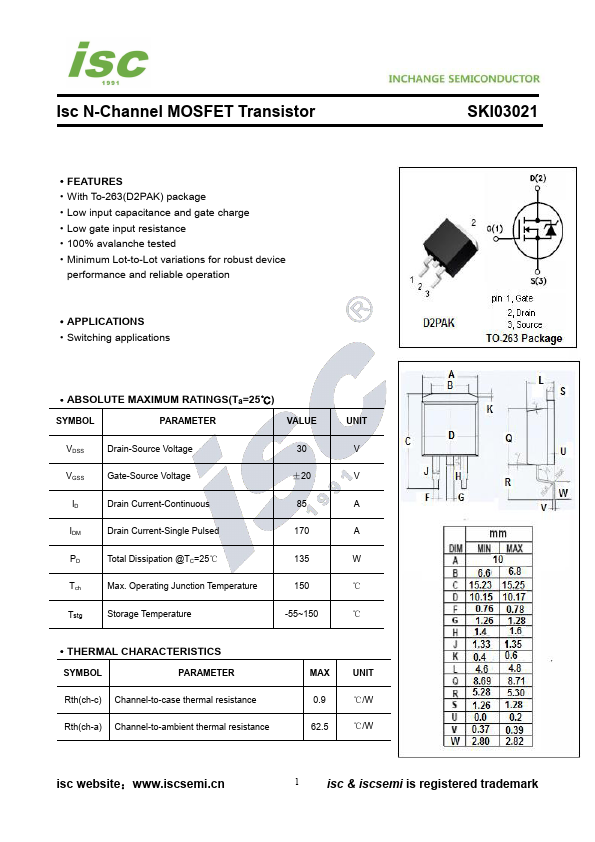
·FEATURES ·With To-263(D2PAK) package ·Low input capacitance and gate charge ...
Isc N-Channel
MOSFET Transistor
SKI03021
·FEATURES ·With To-263(D2PAK) package ·Low input capacitance and gate charge ·Low gate input resistance ·100% avalanche tested ·Minimum Lot-to-Lot variations for robust device
performance and reliable operation
·APPLICATIONS ·Switching applications
·ABSOLUTE MAXIMUM RATINGS(Ta=25℃)
SYMBOL
PARAMETER
VALUE
VDSS
Drain-Source
Voltage
30
VGSS
Gate-Source
Voltage
±20
ID
Drain Current-Continuous
85
IDM
Drain Current-Single Pulsed
170
PD
Total Dissipation @TC=25℃
135
Tch
Max. Operating Junction Temperature
150
Tstg
Storage Temperature
-55~150
UNIT V V A A W ℃ ℃
·THERMAL CHARACTERISTICS
SYMBOL
PARAMETER
Rth(ch-c) Channel-to-case thermal resistance
Rth(ch-a) Channel-to-ambient thermal resistance
MAX 0.9 62.5
UNIT ℃/W ℃/W
isc website:www.iscsemi.cn
1 isc & iscsemi is registered trademark
Isc N-Channel
MOSFET Transistor
ELECTRICAL CHARACTERISTICS
TC=25℃ unless otherwise specified
SYMBOL
PARAMETER
CONDITIONS
BVDSS
Drain-Source Breakdown
Voltage VGS=0V; ID=0.1mA
VGS(th)
Gate Threshold
Voltage
VDS=VGS; ID=1.5mA
RDS(on) Drain-Source On-Resistance
VGS= 10V; ID=110A
IGSS
Gate-Source Leakage Current
VGS= ±20V;VDS=0V
IDSS
Drain-Source Leakage Current VDS=30V; VGS= 0V
VSDF
Diode forward
voltage
ISD=110A, VGS = 0V
SKI03021
MIN TYP MAX UNIT
30
V
1.0
2.5
V
2.1
2.6
mΩ
±0.1 μA
100 μA
0.9
1.5
V
NOTICE: ISC reserves the rights to make changes of the content herein the datasheet at any time w...